Inside ATI & NVIDIA: How they make frames fly
by Anand Lal Shimpi on September 23, 2002 2:14 AM EST- Posted in
- GPUs
Probing, FIBing, & Verifying chips
Our final stop on the engineering portion of the tour took us through one of NVIDIA's low-level testing labs; these labs take silicon after they come back from the fab and are used to test the chips to make sure they function as expected. There was a good deal of equipment in this particular facility for diagnosing defects as well as implementing minor fixes through a FIB tool.
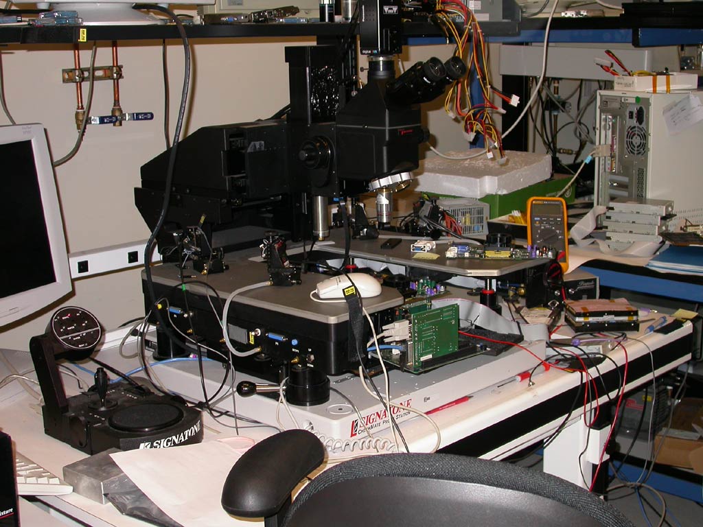
Here (above) you can see some of the probing equipment setup to diagnose low-level chip problems before sending them to the appropriate part of the lab for either further diagnostics or repairs.
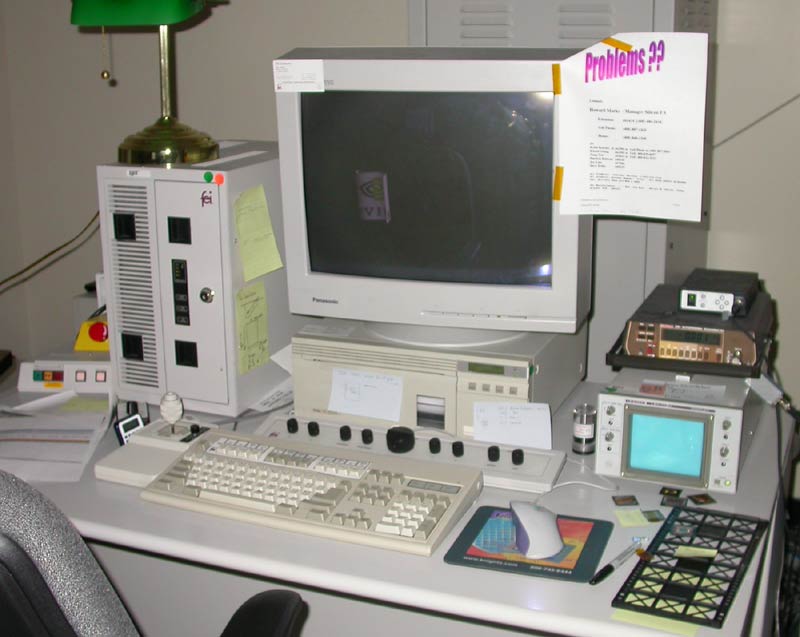
This computer (below) controls the FIB (Focused Ion Beam) tool in the room; as you'll remember from our description at the beginning of this article, the FIB tool can be used to fix minor bugs on silicon without ruining the chip thus saving time and money by not forcing a new spin of the chip.
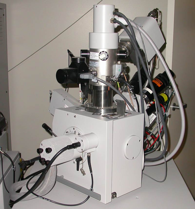
Here's the actual FIB tool itself:
Just across the room from the FIB tool was another very interesting device that is used for probing defects on a chip:
The machine pictured above will actually break down the atomic composition of any material placed in the machine. While the device inevitably gets used for things like random rocks found around on the way to work, its primary use is in finding the cause of defects. Let's take the following picture for example:
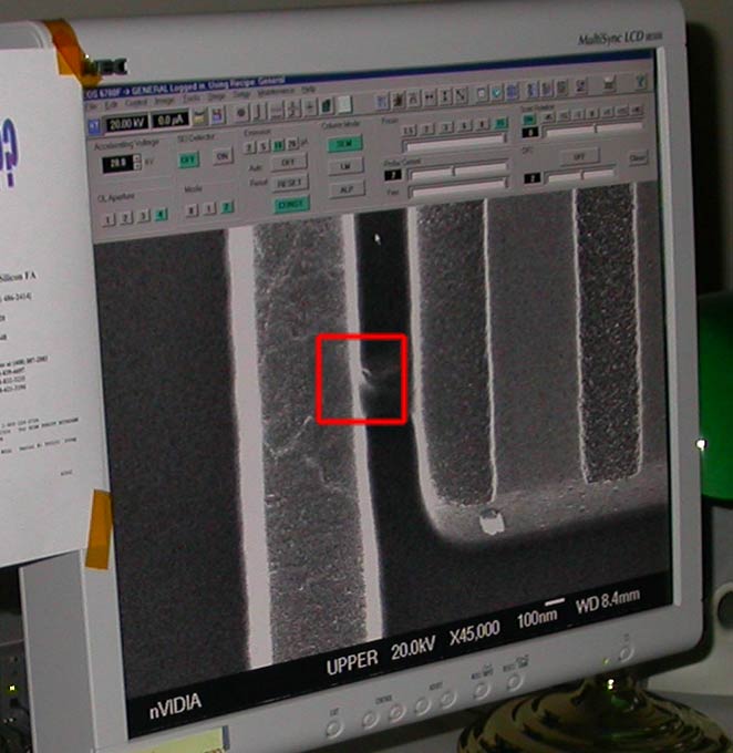
What you see on the screen is a part of a NVIDIA chip magnified at 45,000X its normal size; we've added in the box in red that encloses a defect in the chip itself. This defect could be the result of a problem during manufacturing and the way NVIDIA diagnoses exactly what caused it is by putting the chip through this machine and finding out what the atomic composition of that particular defect is. By finding out the nature of the foreign elements present at that particular point in the silicon you can then figure out what introduced the element to that part of the chip and thus help avoid future defects and improve yields.
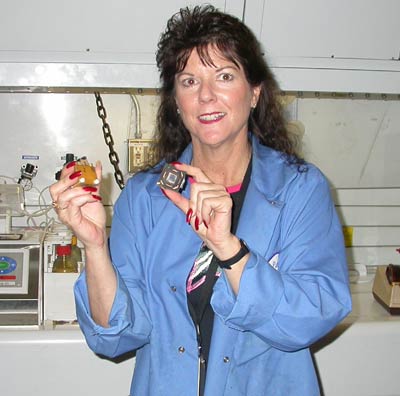
Here we have Patricia, one of the Sr. engineers at NVIDIA that works in this particular lab. In her hands she's holding two chips; in her left hand is a GPU with the top layers of the silicon dissolved and in the right hand is a piece of silicon extracted from the GPU. Below you can see a close-up of the two:
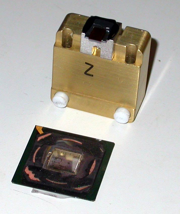
The GPU's core is dissolved using some very powerful acids that it is exposed to in order to gain access to the part of the silicon necessary for removal.
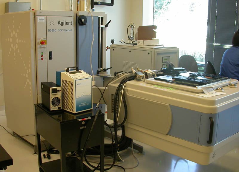
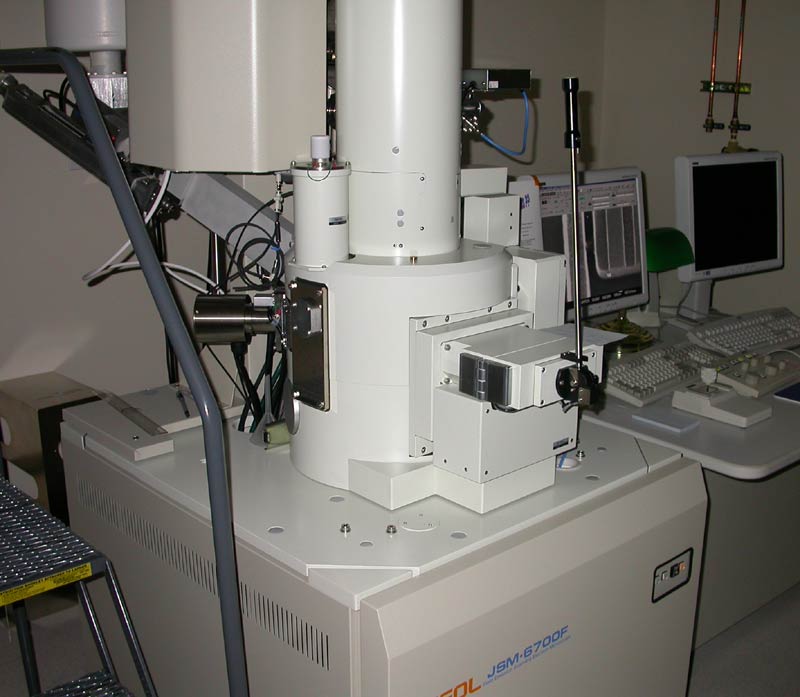
The machine above is a tool used to verify the packaged silicon by running a series of tests to make sure it works according to spec. In chip design there's an incredible amount of emphasis on verification because every bug discovered before spinning a new revision of the silicon saves time and money.


0 Comments
View All Comments