SuperComputing 15: Intel’s Knights Landing / Xeon Phi Silicon on Display
by Ian Cutress on November 19, 2015 2:45 PM EST- Posted in
- CPUs
- Intel
- HPC
- Enterprise
- Trade Shows
- Xeon Phi
- 14nm
- Knights Landing
- SC15
There are lots of stories to tell from the SuperComputing 15 conference here in Austin, but a clear overriding theme – in order to reach ‘Exascale’ (the fancy name given to where a supercomputer hits one ExaFLOP, 1018 FLOPS, in LINPACK), PCIe co-processors and accelerators are going to be a vital aspect in that. Looking at the Top500 supercomputers list that measures supercomputers in pure FLOPS, or the Green/Graph 500 lists that focus on FLOPS/watt and graph compute performance respectively (graph compute such as social networking linked lists of users (nodes) and relationships (edges)), it is clear that focused silicon is key to get peak performance and performance per watt. That focused silicon is often around NVIDIA’s Tesla high performance computing cards, FPGAs (field programmable gate arrays) from Xilinx or Altera, focused architecture designs such as PEZY, or Intel’s Xeon Phi co-processing cards.
We’ve reported on Xeon Phi before, regarding the initial launch of the first generation Knights Corner (KNC) with 6GB, 8GB or 16GB of onboard memory. These parts are listed on Intel's ARK at $1700 to $4150 (most likely less for bulk orders) but KNC forms the backbone of the compute behind the world’s number 1 supercomputer, the Tianhe-2 in China. Over the course of SC15, more details have emerged about the 2nd generation, Knights Landing (KNL) regarding availability and memory configuration, using up to 16GB of onboard high-bandwidth memory using a custom protocol over Micron’s HMC technology and eight onboard HMC memory controllers.

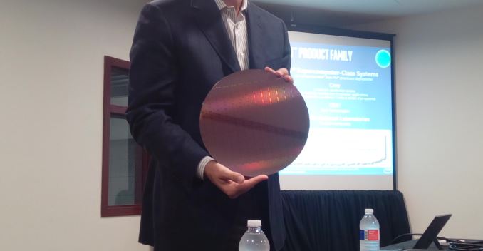
As part of a briefing at SC15, Intel had a KNL wafer on hand to show off. From this image, we can see about 9.4 dies horizontally and 14 dies vertically, suggesting a die size (give or take) of 31.9 mm x 21.4mm, or ~683 mm2. This die size comes in over what we were expecting, but comes in line with other predictions about the route of the first gen, Knights Corner, at least. Relating this to transistor counts, we have a differing story of Charlie Wuischpard (VP of Intel’s Data Center Group) stated 8 billion transistors to us at the briefing but there are reports of Diane Bryant (SVP / GM, Data Center Group) stated 7.1 billion at an Intel Nov ’14 investor briefing, but we can only find one report of the latter. This would come down to the wobbly metric of 10.4-11.7 million transistors per square millimeter.
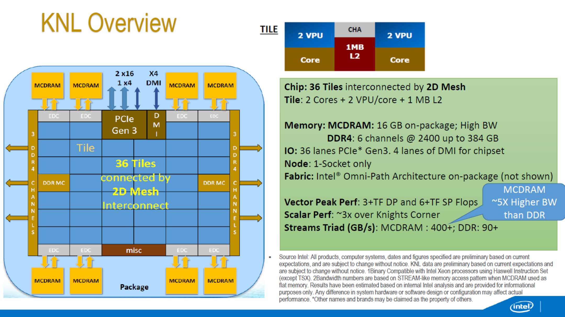
The interesting element about KNL is that where the 1st generation KNC was only available as a PCIe add-in coprocessor card, KNL can either be the main processor on a compute node, or as a co-processor in a PCIe slot. Typically Xeon Phi has an internal OS to access the hardware, but with this new model it eliminates the need for a host node – placing a KNL in a socket will give it access to both 16GB of high speed memory (the MCDRAM) as well as six memory channels for up to 384GB of DDR4, at the expense of the Intel Omni-Path controller. The KNL will also have 36 PCIe lanes which can host two more KNC co-processor cards and another four for other purposes.
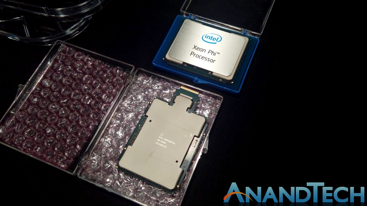
As you might expect, due to the differences we end up with the same die on different packages – one as a processor (top) and one as a co-processor which uses an internal connector for both data and Omnipath. Given the size of the die and the orientation of the cores in the slide above (we can confirm based on the die that it’s a 7x6 arrangement taking into account memory controllers and other IO), the fact that the heatspreader over the package is in a non-rectangular shape is due to the MCDRAM / custom-HMC high speed memory.
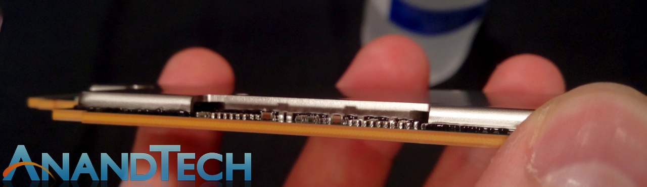
If we look into the side, the headspreader clearly does not go down onto the package all the way around, in order to deal with the on-package memory.
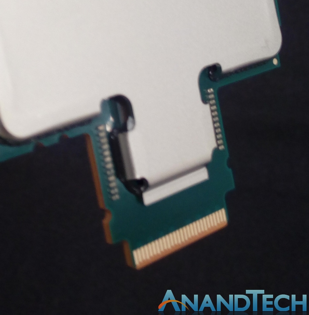
The connector end of the co-processor has an additional chip under the heatspreader, which is most likely an Intel Omni-Path connector or a fabric adaptor for adjustable designs. This will go into a PCIe card, cooler applied and then sold.

The rear of the processor is essentially the same for both.
When it comes to actually putting it on a motherboard, along with the six channels of DDR4, we saw Intel’s reference board on the show floor as a representation on how to do it. A couple of companies had it on display, such as Microway, but this is a base board for others such as Supermicro or Tyan to build on or provide different functionality:

The board is longer than ATX, but thinner. I can imagine seeing one of the future variants of this in a half-width 1U blade with all six channels and two add-in boards, pretty easily. This might give six KNL in a 1U implementation, as long as you can get rid of the heat.
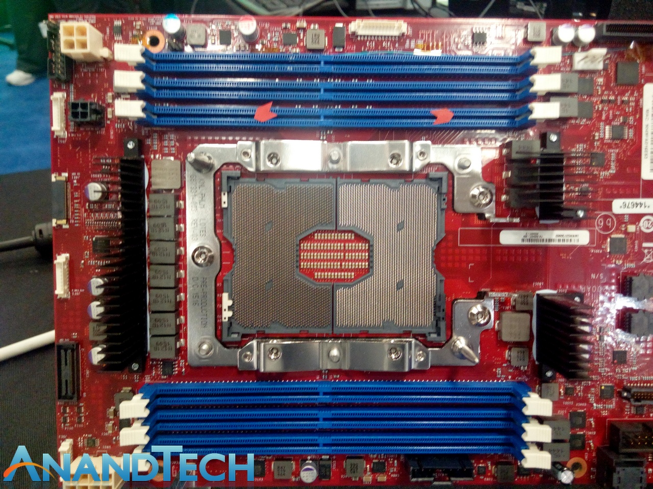
The socket was fairly elaborate, and it would come across that Intel has a high specification on specific pressure for heatsinks . But it is worth noting that the board design does not have an Omni-Path connection, and thus for a server rack then either additional KNLs should be added or PCIe Omni-Path cards need to be added. But this setup should help users wanting to exploit Xeon Phi in a single 1P node and MCDRAM, running the OS on the Xeon Phi itself without MPI commands to use extra nodes. There seems to be a lot of the HPC community here at SC15 who are super excited about KNL.
Regarding availability of Knights Landing, we were told that Intel has made sales for installs in Q4, but commercial availability will be in Q1. We were also told to expect parts without MCDRAM as well.
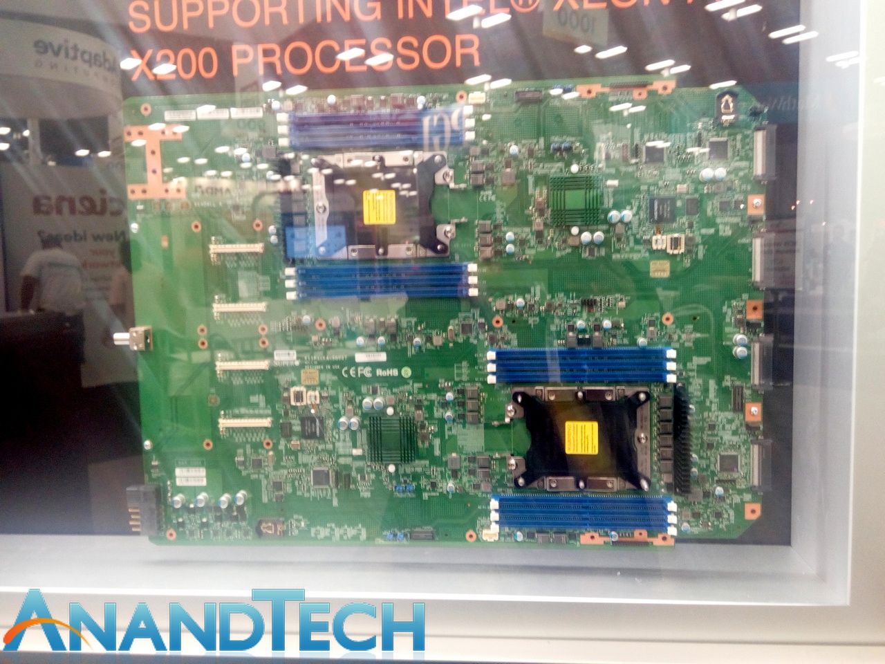
Additional: On a run through the SC15 hall, I caught this gem from SGI. It's a dual socket motherboard, but because KNL processors have no QPI links and can only in 1P systems, this would be equivalent of two KNL nodes in one physical board. Unfortunately they had a plastic screen in front, which distorts the images.


26 Comments
View All Comments
LukaP - Thursday, November 19, 2015 - link
Just noticed lots of mixups of KNL with KNC in the third paragraph. Nice article.LukaP - Thursday, November 19, 2015 - link
Just realised this sounds incredibely sarcastic, its a genuine nice article. Hopefully we will see some more sales of these parts like the one that happened last year. Would love to play with this beast. (and AVX512 is also nice to have)Ian Cutress - Thursday, November 19, 2015 - link
Bleh, mental mixup. Thanks for the heads up :) I'm wondering how easy it would be to run our Linux testing suite on the processor part and if it's just as plug as play as we do now. I suspect not, but I can hope.LukaP - Thursday, November 19, 2015 - link
Well the PCIe ones need extra libraries for openMP IIRC, but one of the major points of the socketed one is that you should in theory not need anything, as its just an "ordinary" CPU, with a DMI link to the chipset, so (again in theory) any x86 OS should work on it.It would be very interesting seeing benchmarks over some vector data for AVX2 vs 512 too understand more about its implementation.
ats - Friday, November 20, 2015 - link
Should be plug and play as long as you don't use an ISA subset that isn't supported.And FYI, I think you have the configurations a bit off. Pretty sure the OPI variant of KNL can be socketed. In fact I'm pretty sure that's the only option for that one as the on package KNL/OPI link takes up the majority of the PCIe lanes. Its also fairly obvious that the socket you are showing has the specific keepaways for the OPI variant as well.
Ian Cutress - Friday, November 20, 2015 - link
You are right, I didn't think of that. Seems like it requires an internal ribbon connector as a result though - I don't think they'd have a physical place to slot it in as well as dealing with a socket.ats - Friday, November 20, 2015 - link
yeah, it is a ribbon connector into the phy cage. AFAICT, they are still using the 100G/4x25G signalling/phy standard (just like Bull is with their new 100G interconnect as well and really for that matter just like EDR IB).Ian Cutress - Saturday, November 21, 2015 - link
http://www.anandtech.com/show/9561/exploring-intel...Might answer some of the signalling questions.
MrSpadge - Thursday, November 19, 2015 - link
Interesting stuff and nice article, indeed!When ever I read something about KNL I get the feeling of wanting a pack of those cores as co-processors in my i7 instead of a beefier GPU. My Skylake GPU is doing 24/7 number crunching, but it's a lot more complicated than with even AMD GPUs, because - frankly - nobody cares about writing and maintaining that openCL software. Let alone dealing with the bugs in Intels driver (e.g. Einstein@Home still doesn't work on Skylake at all). If KNL cores were really as simple to use they'd be better suited than a GPU to what I want to do with them.
MrSpadge - Thursday, November 19, 2015 - link
-> "... as simple to use as Intel claims..."