Intel's 3D NAND to Ship in H2'15: 256Gbit Die & 32 Layers
by Kristian Vättö on November 25, 2014 5:20 AM EST
Last Thursday in its annual Investor Meeting Intel revealed the first details of its 3D NAND technology and announced that it will begin the shipments of 3D NAND in the second half of 2015. While Intel's investment in 3D NAND hasn't been a secret, the company has been relatively quiet about any specifics and the vital specs such as the number of layers and die capacity have remained unknown. In Thursday's webcast, Rob Crooke, Senior VP and General Manager of Intel's non-volatile memory group, disclosed that Intel's first generation 3D MLC NAND die will be 256Gbit (32GB) in capacity and will consist of 32 layers. The technology also enables a 384Gbit (48GB) TLC (3-bit-per-cell) die as we have learned over the years.
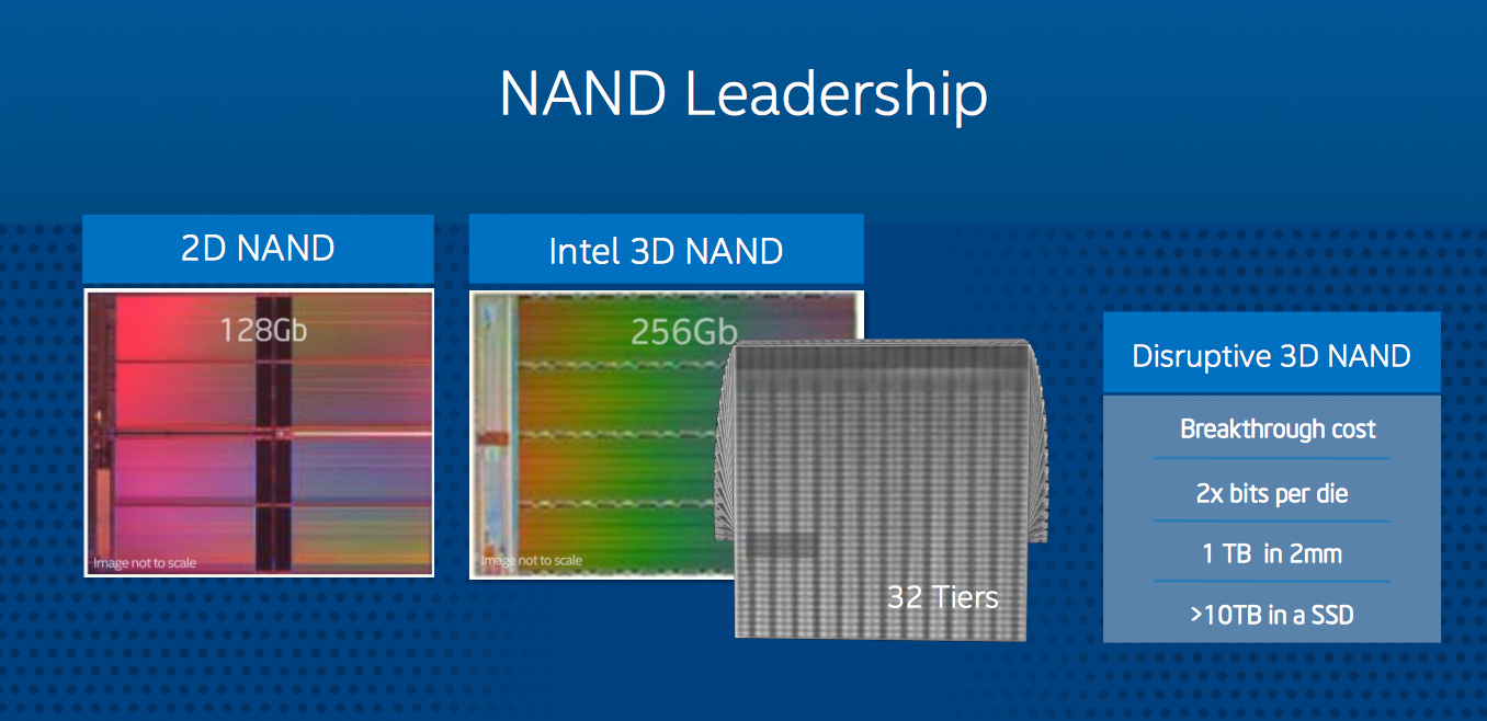
Intel claims that its 3D NAND is the most cost effective on the market and bases this on the fact that its die is 256Gbit whereas Samsung's is only up to 128Gbit at the moment. I'm not sure if I buy Intel's claim because while it's true that a higher capacity die results in higher array efficiency (i.e. peripheral circuitry takes less area), Samsung consciously went from a 24-layer 128Gbit MLC die to a 32-layer 86Gbit MLC die. In other words, Samsung could have upped the die capacity to ~170Gbit by just adding the extra layers, but the company chose to go with a smaller die instead. Smaller capacity dies have advantages in performance (higher parallelism) and applicability because eMMC/microSD devices have very strict die size constraints, so that might be a part of the reason why Samsung's strategy is so different from Intel's and Micron's.
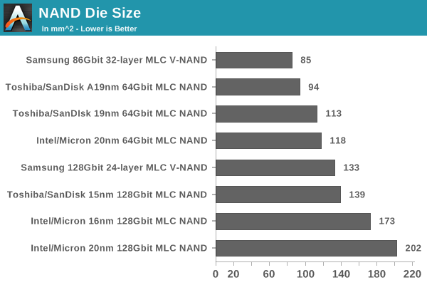
As the graph above shows, Intel's/Micron's NAND dies have historically been larger than the competitors', so the die capacity alone isn't enough to dictate whether Intel's 3D NAND is more cost efficient than Samsung, especially because both have 32 layers. Unlike Samsung, Intel didn't reveal the lithography that is used to manufacture the 3D NAND, but I would say it's safe to assume that the lithography is in the order of 30nm or 40nm because the whole idea of 3D NAND is to move away from multi-patterning to cut costs and with today's technology the smallest pitch of single-patterning is somewhere between 30nm and 40nm. Either way, it will be very interesting to see how Intel's 3D NAND stacks up against Samsung's because there are also some structural differences that affect the production cost as well as performance and endurance, but I'll save the structural analysis for a future article.
Intel said that 3D NAND technology will enable +10TB SSDs in the 'next couple of years', but it wasn't clear whether that is with first generation 3D NAND or some later generation with more layers and higher die capacity. Currently Intel's lineup tops out at 2TB (P3700 & P3600) with a 128Gbit die, so the 256Gbit die alone isn't enough to bring the capacities above 10TB. With effective controller development it should certainly be possible to build a 10TB SSD with a 256Gbit die, although I'm still inclined to believe that Mr. Crooke was referring to second or third generation 3D NAND with his statement.
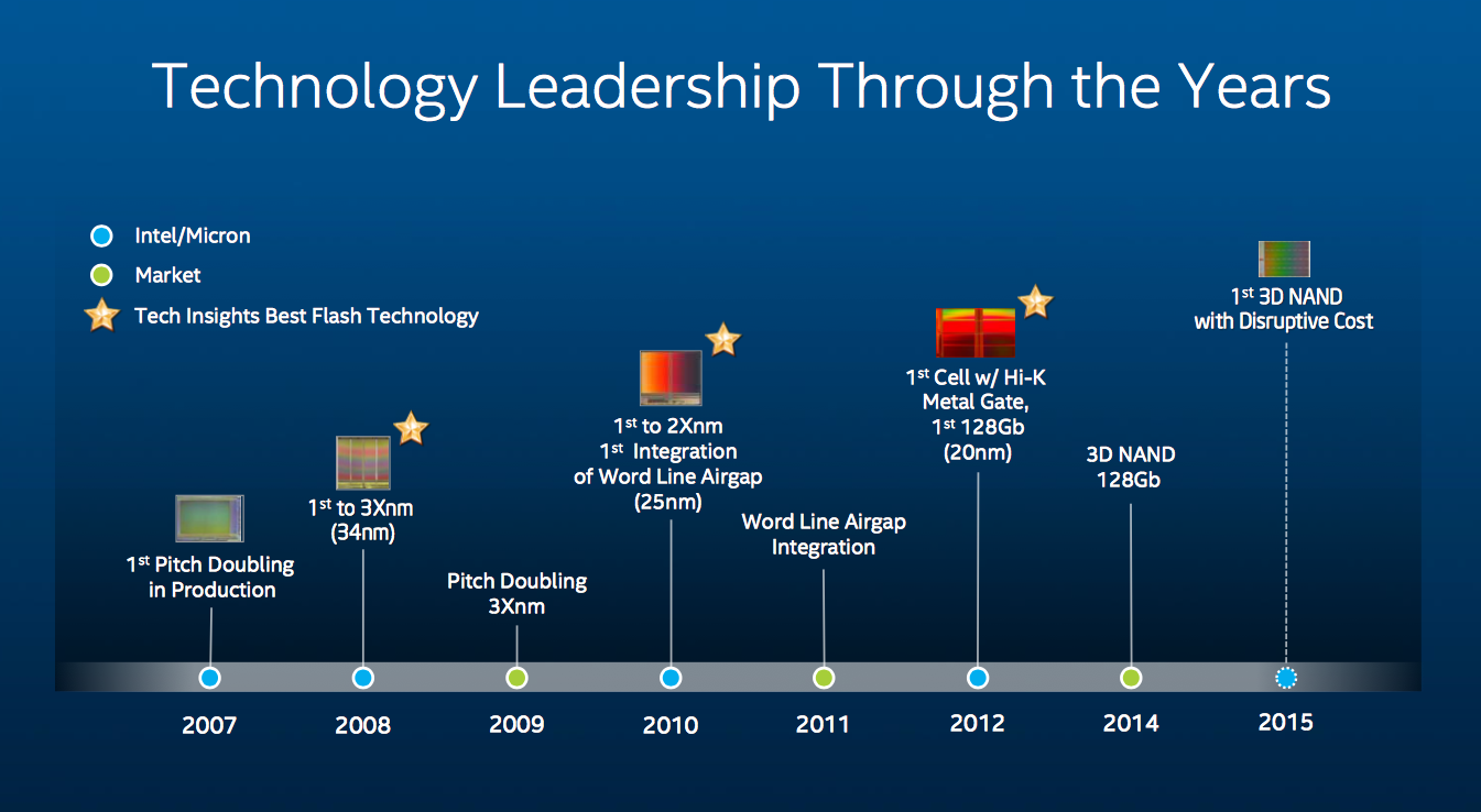
Similar to Intel's previous NAND efforts, 3D NAND has been jointly developed with Micron and will most likely be manufactured in the co-owned Utah plant as Intel sold its share in other fabs a couple of years ago. Interestingly enough, Mr. Crooke said that they also have the ability to bring 3D NAND production to an Intel fab, although to me that sounded more like a statement of technological possibility rather than a hint of future strategy. I wouldn't rule it out, though, but like Mr. Crooke said in the Q&A, Intel needs to have significant competitive advantage for it to make sense. In the past Intel's NAND technologies have generally been slightly ahead of the rest of the industry, but at least as of now Intel doesn't seem to have any substantial advantage in 3D NAND technology as Samsung is already shipping a 32-layer die and will likely ship a 48-layer die before Intel ships its 32-layer product.
All in all, we'll likely get more crumbs of information as the second half of 2015 gets closer. Given Intel's recent SSD strategy, I expect 3D NAND to first find its way to enterprise-class SSDs, but we'll see soon enough.


58 Comments
View All Comments
lilmoe - Tuesday, November 25, 2014 - link
"so the 256Gbit die alone isn't enough to bring the capacities above 10TB"But we still don't know what the actual die size will be. Samsung's 3D-NAND is at 40nm, and the manufacturing process might be slightly different.,I believe (logically speaking) that a node shrink on a 3D-NAND die should see relatively much more gains in area than shrinking nodes for traditional NAND... It'll be interesting to see how things turn out (size/area/performance/endurance VS Samsung's) because 3D-NAND is MUCH more flexible in density, process and area, unless there's something I'm not getting here.
Kristian Vättö - Tuesday, November 25, 2014 - link
The die size isn't really an obstacle when it comes to increasing SSD capacities. The limits lie in die stacking and controller tech as only a limited number of die can be stacked (at least economically) and controllers have a fixed number of die that they can access. That's why the capacity per die is so important as doubled die capacity practically means doubled SSD capacity.We likely won't see traditional die shrinks (i.e. transitions to smaller lithography) with 3D NAND, but just more layers stacked on top of each other.
close - Tuesday, November 25, 2014 - link
The 34nm node is about the most cost effective process right now. Small enough to get a good transistor density but not so small that it requires more expensive techniques to produce. So we may very well see process shrink in the near future, combined with more die stacking.III-V - Tuesday, November 25, 2014 - link
Source? Honestly, that sounds ridiculous. The entire point of moving to higher densities is for the improved economics.garadante - Tuesday, November 25, 2014 - link
Did you not read the article? 3x nm processes are cheaper to produce than smaller nodes in that they're less complex ie using only single patterning. Smaller nodes have historically been economical only because everything is 2D and it allows for more useable product per wafer. 3D technologies have entirely different economics because die size no longer directly correlates to density. Now you have die layers contributing to density. Not to mention larger node NAND has better performance and endurance meaning you save space by needing fewer channels/less spare area for equivalent performance to a smaller node.MrSpadge - Tuesday, November 25, 2014 - link
Ridiculous? That's exactly why the GPUs are still at 28 nm, despite 20 nm being available at TSMC.TelstarTOS - Friday, December 5, 2014 - link
It's not that simple with big die sizes such as GPU...saratoga3 - Tuesday, November 25, 2014 - link
You wouldn't realize it just looking at Intel and ARM processors, but 28 nm will probably the last die shrink for most products for many, many years due to lack of cost effectiveness. One projection I saw shows 28 nm ramping up until the middle of next decade. If you can stay above 30 nm, most products are going to try. 3D NAND is one way to do so.close - Wednesday, November 26, 2014 - link
As I just said, moving to smaller nodes involves technical challenges that exponentially increase costs. Moreover, when it comes to NAND, going to a smaller process cuts your P/E cycles so the endurance drops a lot. Going back to 32/34nm doubles the endurance of today's NAND so you have TLC with MLC endurance. Also the wear leveling algorithms can be simpler.Shrinking is great for 2D NAND because it's the only way to increase the chip's density even if it comes with caveats (like increased costs and reduces endurance). But for 3D NAND it's pointless because you can get the best of both worlds: endurance and cost effectiveness of 3xnm and the density you get from stacking more layers. No need to shrink.
Samus - Tuesday, November 25, 2014 - link
Well it's good to hear they're only a year or so behind Samsung.