The Future of CPU Packaging: Intel's BBUL
by Anand Lal Shimpi on October 8, 2001 8:30 PM EST- Posted in
- CPUs
Getting the Word Out
When taking you through the anatomy of a processor's package we actually identified a key problem with current packaging methods, a limit on the number of flip chip bumps that can be used to connect the silicon to the substrate. This won't become a limitation that will halt microprocessor production anytime soon, but it will be in a few years. We'll get to solutions to this problem later though.
So now that we know how the data being calculated makes its way from the processor to the substrate (through the use of flip-chip bumps), how does it get from there to the rest of your system? The only way out of the chip is through the hundreds of pins on the bottom of the CPU, but before signals can get to the pins they must travel from the silicon through the packaging.
Provided by Intel Corporation
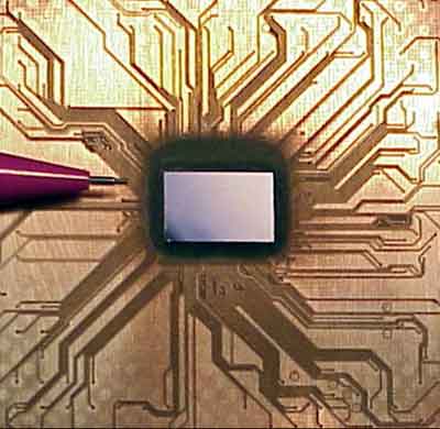
For this example we'll take a FC-PGA (Flip Chip Pin Grid Array) Pentium III processor since you can actually see the lines on the top of the chip. As CPUs become more complex and the silicon decreases in size (smaller manufacturing processes) it's going to become very expensive and very difficult to layout the routing lines coming from the silicon and extending throughout the package.
The next limitation is actually on the inside of the package itself; the silicon is on top, and the pins are on the bottom meaning that the signals from the core have to somehow travel through the packaging to get to the pins. If we were to cut through the substrate and magnify the cross-section of the package we'd see a layered diagram much like the picture below.
At the top are the chip attach pads that connect to the solder points on the silicon. At the bottom we have the spaces for pins; and in the middle of this sandwich we have what are known as micro-vias (sometimes just called vias for short). These micro-vias literally connect the top to the bottom of the package. Today's processors are approaching 10,000 micro-vias in their packages; it won't be too long (a few years) before we have 3 - 5x as many micro-vias inside the package.


4 Comments
View All Comments
Googer - Sunday, January 16, 2005 - link
I cannot beleive after 4 years no one has chosen to comment on such important technology such as this. As of right now Intel has chosen to delay the future of this technology.VasileRT - Thursday, August 19, 2010 - link
It seems that Intel is finally geting started on this. They are currently hiring for this project.extide - Monday, September 10, 2012 - link
It is kinda interesting to read this article 11 years later, and see how things have changed. See what stuff came true and what didn't :)Piyush patel - Thursday, March 21, 2019 - link
Nice post also know about the cpu packaging <a href="https://www.cyberlearningservices.com/2019/03/cpu-... Click Here <\a>.