Imagination's PowerVR Rogue Architecture Explored
by Ryan Smith on February 24, 2014 3:00 AM EST- Posted in
- GPUs
- Imagination Technologies
- PowerVR
- PowerVR Series6
- SoCs
Technical Comparisons
Finally, to close out this look at the Rogue architecture we wanted to spend a bit of time looking at how it compares to other architectures. Unfortunately the lack of details we have on other SoC GPU architectures means we can’t make any meaningful comparisons there beyond the GFLOPs comparisons we do today (and that says nothing of real world efficiency). But we can compare it to the next best thing, which is mobile parts based on desktop GPU architectures from AMD and NVIDIA. The latter case being especially interesting, as we know Kepler will be coming to SoCs with the K1.
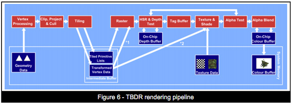
With that said, and we can’t reiterate this enough, this is just a look at theoretical performance. It is not possible to take into account efficiency measures such as memory bandwidth, ROPs, or especially early rejection optimizations such as Tile Based Deferred Rendering. TBDR is Imagination’s ace, and while other GPU firms have their own early rejection technologies, from what little we know about each of them, none of them quite matches TBDR. So Rogue’s theoretical performance aside, if Imagination is rejecting significantly more work before it hits their shaders, then they would have greater performance when all other factors were held equal. The only way to compare the real world performance of these architectures is to benchmark their real world performance, so please do not consider this the final word on performance.
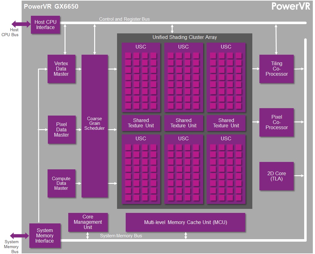
For this comparison we’ll be looking at NVIDIA’s Kepler based K1, AMD’s GCN based A4-1350, and Imagination’s Rogue based GX6650 and G6230. Because Rogue is offered in multiple configurations it’s difficult to determine just how large a Rogue configuration would equal K1 or A4-1350 from a performance and size perspective, but given the anticipated integration time for Series 6XT, a 6 cluster configuration seems the most likely.
| GPU Specification Comparison | |||||||
| NVIDIA K1 | Imagination PVR GX6650 | Imagination PVR G6230 | AMD A4-1350 | NVIDIA GTX 650 | |||
| FP32 ALUs | 192 | 192 | 64 | 128 | 384 | ||
| FP32 FLOPs | 384 | 384 | 128 | 256 | 768 | ||
| Pixels/Clock (ROPs) | 4 | 12 | 4 | 4 | 16 | ||
| Texels/Clock | 8 | 12 | 4 | 8 | 32 | ||
| GFLOPS @ 300MHz | 115.2 GFLOPS | 115.2 GFLOPS | 38.4 GFLOPS | 76.8 GFLOPS | 230.4 GFLOPS | ||
| Architecture | Kepler | Rogue (6XT) | Rogue (6) | GCN 1.0 | Kepler | ||
Briefly, we can see that as far as theoretical shading performance is concerned, both the GX6650 and K1 are neck-and-neck when clockspeeds are held equal. Both of them have the same ILP dependency, so both need to be able to pull off some FP32 co-issued instructions if they are to achieve their full 384 FLOP/cycle throughput. The A4-1350 on the other hand has no such limitation, making it easier to hit its 256 FLOP/cycle throughput, but never getting the chance to go past it.
Meanwhile it was surprising to see that GX6650’s theoretical pixel throughput was so high. 12 pixels/clock (12 ROPs) is much higher than either K1 or A4-1350, and in fact is quite high for an SoC class product. Most designs use relatively few ROPs here for size and power reasons, and not all designs replicate the ROPs with the shader blocks. So having 12 ROPs here was unexpected. At the same time it remains to be seen how well real world efficiency tracks this, as ROPs are frequently memory bandwidth constrained, which makes such a large number of ROPs harder to feed.
Moving on to quickly compare texture throughput, again it’s surprising to see just how many texels GX6650 can push. TMUs regularly scale with shader core counts, so the fact that it’s three-fold what a single TMU design can do is not unexpected, but until now we had never realized just what that meant for overall texture throughput. 12 texels/clock is (thankfully) a lot of texels for a SoC GPU. That said, this is also a memory bandwidth heavy operation, so it’s difficult to say how real world performance will track it.
Finally, to throw in a true desktop comparison for the fun of it, we also put NVIDIA’s Kepler based GTX 650 in the chart. Clockspeeds aside, the best case scenario for even GX6650 is that it achieves half the shading throughput as GTX 650. The ROP throughput gap on the other hand is narrower (but GTX 650 will easily have 2x the memory bandwidth) and the texture throughput gap is nearly 3x wider. In practice it would be difficult to imagine the GX6650 being any closer than about 40% of the GTX 650’s performance, once again owing to the massive memory bandwidth difference between an SoC and a discrete GPU.
Final Words
Wrapping up this architectural overview of Imagination’s Rogue architecture, it’s exciting to finally see much of the underpinnings of an SoC GPU design. While we haven’t seen every facet of Rogue yet – and admittedly it’s unlikely we ever will – the information that we’ve received on Rogue so far has given us a much better perspective on how Imagination’s latest graphics architecture works, and for that matter how Series 6 and Series 6XT differ from one-another.
Ultimately we still can’t do true apples-to-apples comparisons with these integrated GPUs (we can’t separate the CPU and memory controller from the GPU), but it should be helpful for better understanding why certain products perform the way they do, and determining what the stronger products might be in the long run. So it’s with some hope and a bit of luck that this might get the ball rolling with the other SoC GPU vendors, getting them to open up their doors a bit more so that we can see what’s inside their designs.
Coming back full circle to Imagination, we’re left with one of the big reasons why they’re opening up in the first place: core wars. Imagination is keen on not being seen as being left behind on core counts, and while we don’t expect the “core” terminology to go away any time soon, now that we have these low level Rogue architecture details, we can agree that Imagination does have a salient point as far as counting cores and ALUs is concerned.
For the purposes of FP32 operations a Rogue USC is essentially equivalent to a 32 core design, with an ILP reliance similar to what we’re seeing out of NVIDIA right now, though perhaps greater than some other designs. Or as Imagination likes to compare it to, a 6 USC design would be equivalent to a 192 core design. This speaks nothing of real world performance – without real world hardware it can’t, there are too many external variables – but it does give us an idea of how many clusters Imagination’s customers would need to achieve various degrees of theoretical performance, including what it would take to beat the competition.


95 Comments
View All Comments
jjj - Monday, February 24, 2014 - link
Far from ideal timing with so many news around, guess i'll have to read it after MWC.rpg1966 - Monday, February 24, 2014 - link
Thank you for sharing.Mondozai - Monday, February 24, 2014 - link
The most important part is what Anand highlighted from this walkthrough; namely that the Rogue series has a chip that is on equal balance if not even stronger than Tegra K1.Poor Nvidia.
Sabresiberian - Monday, February 24, 2014 - link
That remains to be seen - but it does appear to be competitive at this point. We also don't know what the entire Denver+K1 package will do.What kind of surprises me about K1 though is that Maxwell has already been released for the desktop. I would think "M1" (to guess at a name) would be the architecture to build on in the next year.
dragonsqrrl - Monday, February 24, 2014 - link
Uhhh no it doesn't. The article failed to mention this important piece of information, but you realize the 6XT series probably won't come to market before 2015 right? Likely 2H 2015 according to an earlier article published here on Anandtech.grahaman27 - Monday, February 24, 2014 - link
Interesting. Which article mentioned that? Would you mind linking me to it?I can't find an expected release date for this chip anywhere.
dragonsqrrl - Tuesday, February 25, 2014 - link
That's because there is none. It was an estimate given by Ryan Smith based on prior Imagination GPU announcements, and the time it usually takes chipmakers to integrate the design and bring a device to market."Finally, while Imagination doesn’t provide a timeframe for consumer availability (since they only sell designs to chipmakers), based on the amount of time needed to integrate these designs into new products and then get those products in the hands of consumers, we should be looking at a timetable similar to the original Series6 designs. In which case Series6XT equipped SoCs would start appearing in 2015, likely in the latter half."
http://www.anandtech.com/show/7629/imagination-tec...
michael2k - Tuesday, February 25, 2014 - link
Really? You don't think their biggest customer, Apple, which has shown the ability to beat an entire industry to market by almost a year (64 bit ARMv8) and one of the first PVR6 customers to market as well? Anand though it would be 2014 when PVR6 would show up to market, and the A9600 that was supposed to show up in 2013 never did (Apple's A7 did though!)So why do you rule out the real possibility that the Apple A8 would ship with a 6XT this year?
dragonsqrrl - Tuesday, February 25, 2014 - link
I don't know, ask Ryan Smith.My theory for the ~18 month estimate is that it's about how long Apple took to integrate and bring their current series 6 GPU to market in the A7. I suppose if any company had the resources to accelerate that schedule, it would be Apple. But then the question becomes why and does it make sense? There will be faster Series 6 SKU's available for the A8 in the interim.
stingerman - Wednesday, February 26, 2014 - link
But don't forget, Apple has been involved in this design long before Imagination's public reveal. In fact, Apple informed Imaginations design with their real world experience and their own needs. I always expect Apple to get a 6 to 12 month lead. And, Apple has shown themselves to put a very high value on their SoC GPU leadership.