AMD Kaveri Review: A8-7600 and A10-7850K Tested
by Ian Cutress & Rahul Garg on January 14, 2014 8:00 AM ESTLlano, Trinity and Kaveri Die: Compared
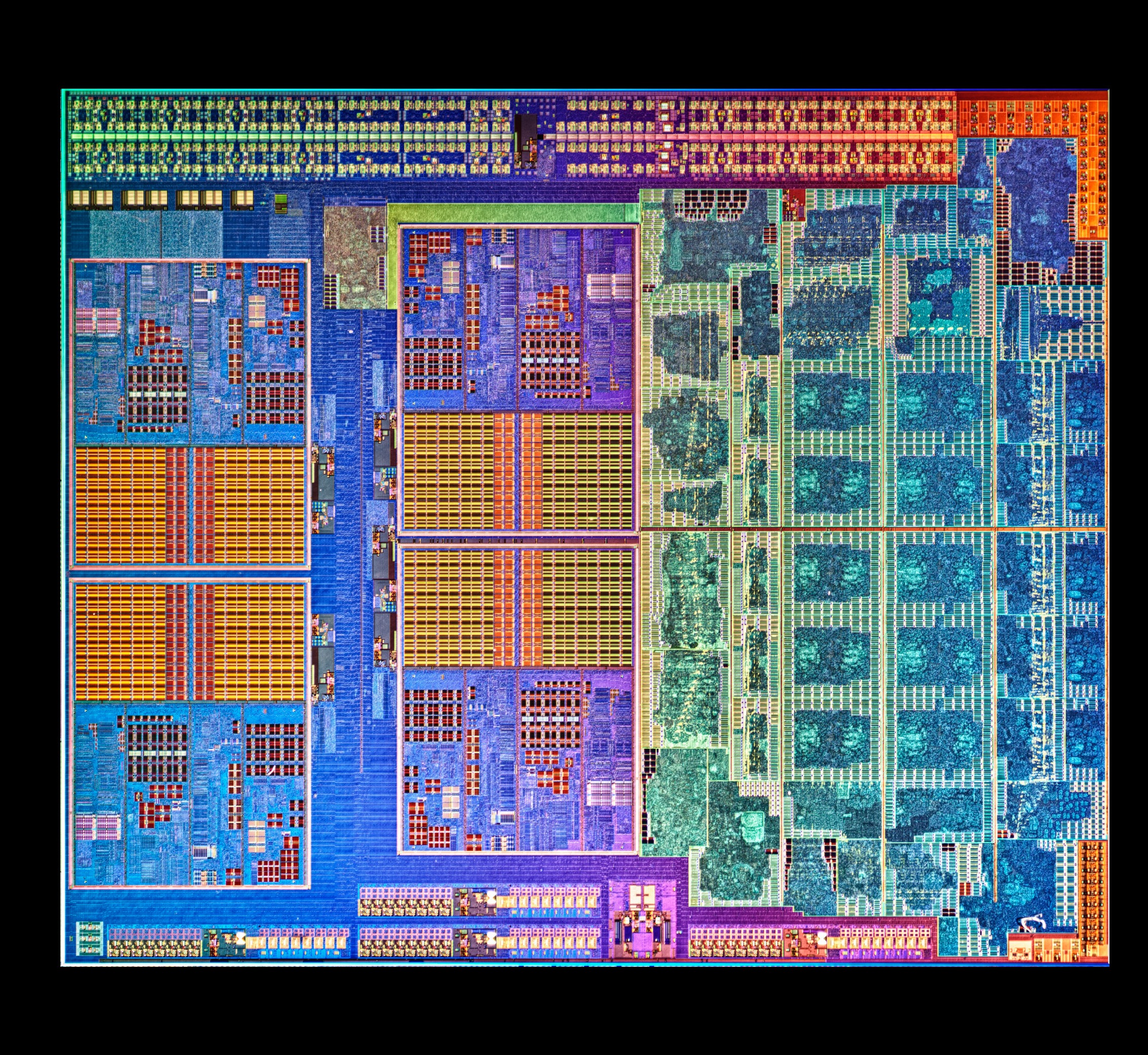
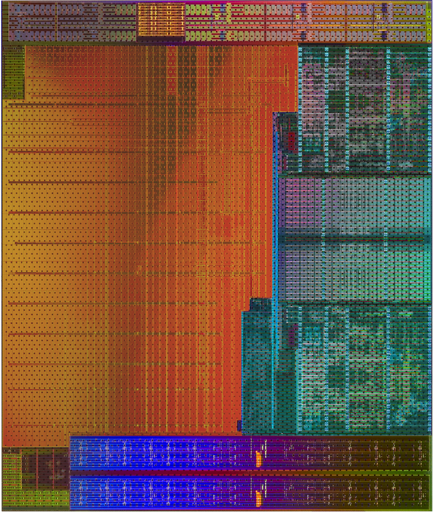
AMD sent along a high res shot of Kaveri's die. Armed with the same from the previous two generations, we can get a decent idea of the progression of AMD's APUs:
Llano, K10 Quad Core

Trinity and Richland Die, with two Piledriver modules and processor graphics
Kaveri, two modules and processor graphics
Moving from Llano to Trinity, we have the reduction from a fully-fledged quad core system to the dual module layout AMD is keeping with its APU range. Moving from Richland to Kaveri is actually a bigger step than one might imagine:
| AMD APU Details | ||||
| Core Name | Llano | Trinity | Richland | Kaveri |
| Microarch | K10 | Piledriver | Piledriver | Steamroller |
| CPU Example | A8-3850 | A10-5800K | A10-6800K | A10-7850K |
| Threads | 4 | 4 | 4 | 4 |
| Cores | 4 | 2 | 2 | 2 |
| GPU | HD 6550 | HD 7660D | HD 8670D | R7 |
| GPU Arch | VLIW5 | VLIW4 | VLIW4 | GCN 1.1 |
| GPU Cores | 400 | 384 | 384 | 512 |
| Die size / mm2 | 228 | 246 | 246 | 245 |
| Transistors | 1.178 B | 1.303 B | 1.303 B | 2.41 B |
| Power | 100W | 100W | 100W | 95W |
| CPU MHz | 2900 | 3800 | 4100 | 3700 |
| CPU Turbo | N/A | 4200 | 4400 | 4000 |
| L1 Cache |
256KB C$ 256KB D$ |
128KB C$ 64KB D$ |
128KB C$ 64KB D$ |
192KB C$ 64KB D$ |
| L2 Cache | 4 x 1MB | 2 x 2 MB | 2 x 2 MB | 2 x 2 MB |
| Node | 32nm SOI | 32nm SOI | 32nm SOI | 28nm SHP |
| Memory | DDR-1866 | DDR-1866 | DDR-2133 | DDR-2133 |
Looking back at Llano and Trinity/Richland, it's very clear that AMD's APUs on GF's 32nm SOI process had a real issue with transistor density. The table below attempts to put everything in perspective but keep in mind that, outside of Intel, no one does a good job of documenting how they are counting (estimating) transistors. My only hope is AMD's transistor counting methods are consistent across CPU and GPU, although that alone may be wishful thinking:
| Transistor Density Comparison | ||||||||
| Manufacturing Process | Transistor Count | Die Size | Transistors per mm2 | |||||
| AMD Kaveri | GF 28nm SHP | 2.41B | 245 mm2 | 9.837M | ||||
| AMD Richland | GF 32nm SOI | 1.30B | 246 mm2 | 5.285M | ||||
| AMD Llano | GF 32nm SOI | 1.178B | 228 mm2 | 5.166M | ||||
| AMD Bonaire (R7 260X) | TSMC 28nm | 2.08B | 160 mm2 | 13.000M | ||||
| AMD Pitcairn (R7 270/270X) | TSMC 28nm | 2.80B | 212 mm2 | 13.209M | ||||
| AMD Vishera (FX-8350) | GF 32nm SOI | 1.2B | 315 mm2 | 3.810M | ||||
| Intel Haswell 4C (GT2) | Intel 22nm | 1.40B | 177 mm2 | 7.910M | ||||
| NVIDIA GK106 (GTX 660) | TSMC 28nm | 2.54B | 214 mm2 | 11.869M | ||||
If AMD is indeed counting the same way across APUs/GPUs, the move to Kaveri doesn't look all that extreme but rather a good point in between previous APUs and other AMD GCN GPUs. Compared to standalone CPU architectures from AMD, it's clear that the APUs are far more dense thanks to big portions of their die being occupied by a GPU.


380 Comments
View All Comments
geniekid - Tuesday, January 14, 2014 - link
Would've been nice to see a discrete GPU thrown in the mix - especially with all that talk about Dual Graphics.Ryan Smith - Tuesday, January 14, 2014 - link
Dual graphics is not yet up and running (and it would require a different card than the 6750 Ian had on hand).Nenad - Wednesday, January 15, 2014 - link
I wonder if Dual Graphics can work with HSA, although I doubt due to cache coherence if nothing else.While on HSA, I must say that it looks very promising. I do not have experience with AMD specific GPU programming, or with OpenCL, but I do with CUDA (and some AMP) - and ability to avoid CPU/GPU copy would be great advantage in certain cases.
Interesting thing is that AMD now have HW that support HSA, but does not yet have software tools (drivers, compilers...), while NVidia does not have HW, but does have software: in new CUDA, you can use unified memory, even if driver simulate copy for you (but that supposedly means when NVidia deliver HW, your unaltered app from last year will work and use advantage of HSA)
Also, while HSA is great step ahead, I wonder if we will ever see one much more important thing if GPGPU is ever to became mainstream: PREEMPTIVE MULTITASKING. As it is now, still programer/app needs to spend time to figure out how to split work in small chunks for GPU, in order to not take too much time of GPU at once. It increase complexity of GPU code, and rely on good behavior of other GPU apps. Hopefully, next AMD 'unification' after HSA would be 'preemptive multitasking' ;p
tcube - Thursday, January 16, 2014 - link
Preemtion, dynamic context switching is said to come with excavator core/ carizo apu. And they do have the toolset for hsa/hsail, just look it up on amd's site, bolt i think it's called it is a c library.Further more project sumatra will make java execute on the gpu. At first via a opencl wrapper then via hsa and in the end the jvm itself will do it for you via hsa. Oracle is prety commited to this.
kazriko - Thursday, January 30, 2014 - link
I think where multiple GPU and Dual Graphics stuff will really shine is when we start getting more Mantle applications. With that, each GPU in the system can be controlled independently, and the developers could put GPGPU processes that work better with low latency to the CPU on the APU's built in GPU, and processes for graphics rendering that don't need as low of latency to the discrete graphics card.Preemptive would be interesting, but I'm not sure how game-changing it would be once you get into HSA's juggling of tasks back and forth between different processors. Right now, they do have multitasking they could do by having several queues going into the GPU, and you could have several tasks running from each queue across the different CUs on the chip. Not preemptive, but definitely multi-threaded.
MaRao - Thursday, January 16, 2014 - link
Instead AMD should create new chipsets with dual AMU sockets. Two A8-7600 APUs can give tremendous CPU and GPU performance, yet maintaining 90-100W power usage.PatHeist - Thursday, February 13, 2014 - link
Making dual socket boards scale well is tremendously complex. You also need to increase things like the CPU cache by a lot. Not to mention that performance would tend to scale very badly with the additional CPU cores for things like gaming.kzac - Monday, February 16, 2015 - link
Having 2 or more APUs on a logic board would defeat the purpose of having an APU in the first place, which was to eliminate processing being handled by the logic board controller. With dual APU sockets, there would need to be some controller interjected to direct work to the APUs which could create a bottle neck in processing time (clock cycles). This is the very reason for the existence of multi core APUs and CPUs of today.Its my expectation that we will start to observe much more memory being added to the APU at some point, to increase throughput speeds. Essentially think of future APUs becoming a mini computer within, the only limitations currently to this issue are heat extraction and power consumption.
5thaccount - Tuesday, January 21, 2014 - link
I'm not so interested in dual graphics... I am really curious to see how it performs as a standard old-fashioned CPU. You could even bench it with an nVidia card. No one seems to be reviewing it as a processor. All reviews review it as an APU. Funny thing is, several people I work with use these, but they all have discrete graphics.geniekid - Tuesday, January 14, 2014 - link
Nvm. Too early!