NVIDIA Announces Tegra K1 SoC with Optional Denver CPU Cores
by Anand Lal Shimpi on January 5, 2014 10:55 PM EST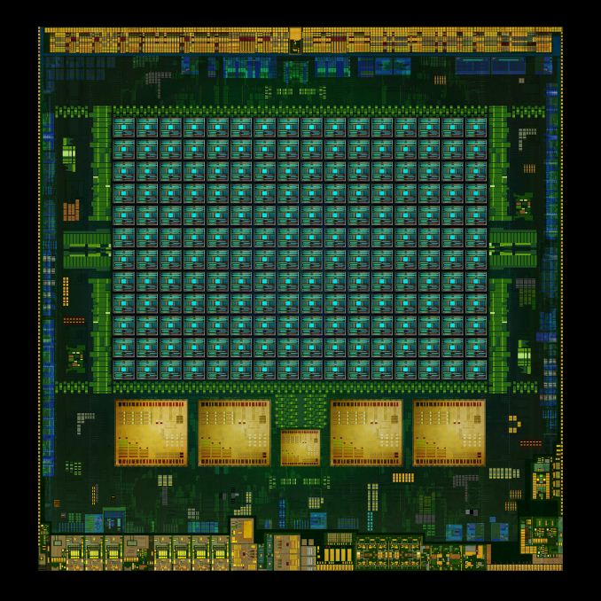
At its CES press conference, NVIDIA finally revealed the marketing name for Project Logan - NVIDIA's latest mobile SoC: Tegra K1.
NVIDIA hasn't said much about the architectural details about its latest Tegra SoC, other than to confirm that it features 192 CUDA cores. Since we already know Tegra K1 is based on NVIDIA's Kepler GPU architecture, and a single Kepler SMX features 192 CUDA cores, we know that K1 uses a single Kepler SMX.
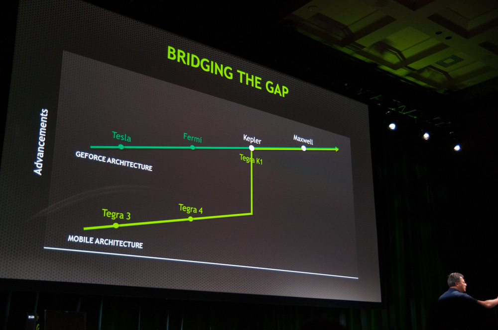
With K1, NVIDIA ditches the GeForce ULP GPU core that was present in the previous four generations of Tegra and moves mobile onto the same roadmap as the desktop/notebook GeForce. NVIDIA used the slide below that seems to imply convergence between the Tegra and GeForce architectures going forward, even beyond Kepler.
We'll be updating this post with more details as NVIDIA reveals them.
Tegra K1 will be available in quad-core Cortex A15 (+1 shadow Cortex A15 core) and dual-core Denver (64-bit ARMv8) versions. The Cortex A15 version will be available in 1H 2014, the Denver version will show up in the second half of 2014.


20 Comments
View All Comments
twotwotwo - Sunday, January 5, 2014 - link
That...is a rather GPU-heavy die shot.tviceman - Sunday, January 5, 2014 - link
About time Nvidia took graphics seriously in mobile!Homeles - Monday, January 6, 2014 - link
Nvidia doesn't really ever show "die shots" of their Tegra line. Everything they show off is doctored to the point where it stops being a die shot and becomes an "artist's representation."Here, for instance, they've copy-pasted some terrible little thumbnail of a "core" to try to portray the (stupid) idea that it's a "192 core processor."
If you can't tell, I'm rather annoyed at Nvidia's decision to alter their die shots so much. Even their flagship GPU die shots are photoshopped worse than adult industry workers. It's been this way since Fermi showed up.
Their Project Denver mockup (http://bit.ly/1d9zCMR) was a chopped up and regurgitated GF100. It's incredibly misleading at best, and false advertising at worst. Nvidia's not alone in this; AMD has done similar things as well (e.g. a supposed Cayman die shot, where a Barcelona die was superimposed on R770), but not nearly to the same extent. Intel also makes heavily-shopped die representations. Nvidia’s by far the worst, though. You’d be best off passing off Nvidia’s official die shots as being fake, because they honestly are.
jasonelmore - Monday, January 6, 2014 - link
i cant tell it's doctored. in fact, if you put took the color out and threw a sephia filter over it, it'd look just like chipworks die shots.psychobriggsy - Monday, January 6, 2014 - link
You only need to look at the fifth CPU core to see that it's a shrunken down image of the other cores. In reality it's either an A7 for the low-power operation, or the fifth core is an A15 and would be roughly the same size at the other A15s.SetiroN - Monday, January 6, 2014 - link
And the fact that YOU can't tell means...?vinayshivakumar - Tuesday, January 7, 2014 - link
Its definitely fake die shots. If its a A7 , it can thav ethe sae exact memory positions and shrunk down sizes. It cant be an A15. I am not sure why they do this....SetiroN - Monday, January 6, 2014 - link
Thankfully, there's chipworks.twotwotwo - Monday, January 6, 2014 - link
Yeah, sort of wonder what the real thing will look like now.chizow - Monday, January 6, 2014 - link
Going to be one seriously fast SoC for the mobile space. Looking forward to seeing some actual designs that use it.