VIA KT266 Socket-A DDR Chipset: Third time's a charm?
by Anand Lal Shimpi on April 10, 2001 3:44 AM EST- Posted in
- CPUs
The Chipset
While the KT266 is VIA's first DDR Athlon chipset, the Apollo Pro266 was actually VIA's first DDR capable chipset, but it was for the Socket-370 platform thus supporting the Intel Pentium III and Celeron processors. The Pro266 was a significant departure from previous VIA chipsets because it introduced a new bus connecting the North and South Bridges in the chipset.
As a quick refresher, the North Bridge is what houses the memory and AGP controllers. It is also the chip that lies connects directly to the CPU, thus controlling your FSB frequency among other things related to your CPU bus interface.
The South Bridge handles any ISA bridges, the integrated hard drive controller, it contains the USB controller and in the case of VIA's 686A, it also houses the keyboard/mouse controllers.
Prior to the Pro266, the North and South Bridges were connected using the 32-bit PCI bus running at 33MHz for a peak theoretical bandwidth of 133MB/s. With current IDE hard drives approaching 40MB/s sustained transfer rates, USB devices becoming increasingly more popular and 100Mbit Ethernet cards eating up this 133MB/s of available bandwidth there is a need to remove this potential bottleneck from the system.
VIA removed this bottleneck through the use of their 8-bit V-Link bus that operates at 266MB/s, identical to the bandwidth offered by Intel's interlink bus. V-Link takes the place of the PCI bus between the North and South Bridges, leaving the PCI bus as an extension off of the South Bridge instead of the path for communication between the two major parts of the chipset.
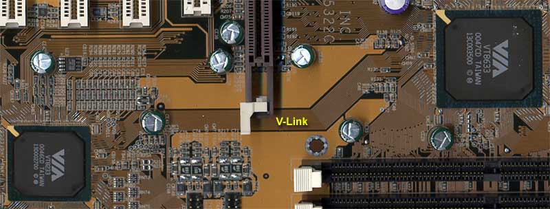
You can easily see the V-Link connection between the North and the South Bridges on the Pro266 Reference board pictured below.
The Apollo Pro266 was the first VIA chipset to feature V-Link, and the KT266 is the second.
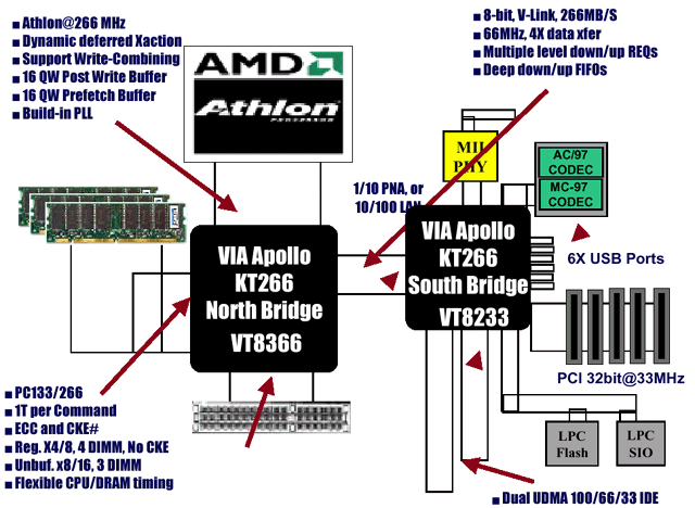
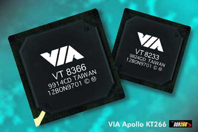
In order to support DDR SDRAM and V-Link, the KT266 must use a different North Bridge from the KT133/A series of chipsets however it can borrow the same 8233 South Bridge from the Apollo Pro266. The KT266 uses the 8366 North Bridge, which offers the same feature-set as the KT133A with the exception of its DDR SDRAM support. This does mean that the North Bridge supports PC133 SDRAM, a feature that you may see some OEMs take advantage of to provide "one-size fits all" motherboard designs.
Since the chipset uses the same 8233 South Bridge as the Pro266, we can quote our Pro266 review in regards to the features it supports:
The South Bridge is virtually identical to the 686B from VIA with the exception that it now contains the PCI bus interface, an integrated 10/100 Ethernet controller and supports up to 6 USB ports.
One of the most attractive selling points the KT266 chipset does have is that it is around 10 - 15% cheaper than the AMD 760. While that doesn't translate into much savings for the consumer, it does help save the motherboard manufacturer quite a bit, making it a very attractive solution for them.


0 Comments
View All Comments