AMD Athlon "Thunderbird" 1.33GHz/1.30GHz
by Anand Lal Shimpi on March 22, 2001 4:52 AM EST- Posted in
- CPUs
The Chips
The reason for launching two CPUs today is simple; since 133MHz DDR FSB platforms, such as the AMD760 and the VIA KT133A, are not too widespread yet AMD has to release both a 133MHz FSB processor and a 100MHz FSB part so that they can offer an even faster performing platform as well as a 100MHz FSB part for compatibility.
If you'll remember, this is actually the opposite of what Intel did when they were ramping up their first 133MHz FSB parts. Instead of continuing to produce 100MHz FSB Pentium IIIs, Intel decided to stop making 100MHz FSB Pentium IIIs faster than 850MHz and focus entirely on 133MHz FSB parts. Later on, after the majority of the market had transitioned to 133MHz platforms, Intel released 900MHz and 1GHz parts that used the 100MHz FSB for late adopters.
It would be advisable for AMD to mimic Intel in this respect if they plan on eventually moving to the 133MHz DDR FSB for all of their Athlon processors, however because AMD does not have a widely available chipset of their own (AMD760 isn't a mass-produced chipset intended for the entire market) that supports the 133MHz FSB this isn't really an option. AMD's continued dependence on ALi, SiS and VIA for the majority of their platforms may end up hurting them in the long run if they ever do decide to take on a more active role as a technology leader in the processor market.
|
CPU
Specification Comparison
|
||||||
|
AMD
Duron
|
AMD
Athlon
|
Intel
Pentium 4
|
Intel
Pentium III
|
Celeron
|
||
|
Core
|
Spitfire
|
Thunderbird
|
Willamette
|
Coppermine
|
Coppermine
128
|
|
|
Clock
Speed
|
600
- 850MHz
|
750
- 1333MHz
|
1.3GHz
- 1.5GHz
|
500
- 1000MHz
|
533
- 800MHz
|
|
|
L1
Cache
|
128KB
|
8KB
Data
|
32KB
|
|||
|
L2
Cache
|
64KB
|
256KB
|
256KB
|
256KB
|
128KB
|
|
|
L2
Cache speed
|
Core
Clock
|
|||||
|
L2
Cache bus
|
64-bit
|
256-bit
|
||||
|
System
Bus
|
100MHz
DDR EV6
|
100/133MHz
DDR EV6
|
100MHz
quad-pumped GTL+
|
100/133MHz
GTL+
|
||
|
Interface
|
Socket-462
(Socket-A)
|
Socket-423
|
Slot-1/Socket-370
|
Socket-370
|
||
|
Manufacturing
Process |
0.18-micron
|
|||||
|
Die
Size
|
100mm^2
|
120mm^2
|
217mm^2
|
106mm^2
|
106mm^2
|
|
|
Transistor
Count
|
25
million
|
37
million
|
42
million
|
28
million
|
28
million
|
|
The 1.33GHz part runs at 1333MHz using a 10.0x clock multiplier and a 133MHz DDR FSB. The 1.30GHz part runs at 1300MHz using a 13.0x clock multiplier and a 100MHz DDR FSB.
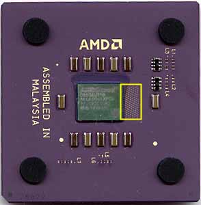
The first thing we noticed about the 1.33GHz part is that the chip has actually changed slightly when compared to previous Athlons. If you'll remember, the Thunderbird core has 256KB of on-die L2 cache compared to the 64KB L2 on the Duron. This makes the Thunderbird core noticeably larger than the Duron core; the difference in size is further illustrated by a pattern of dots to the right of the core. The above picture provides the comparison.
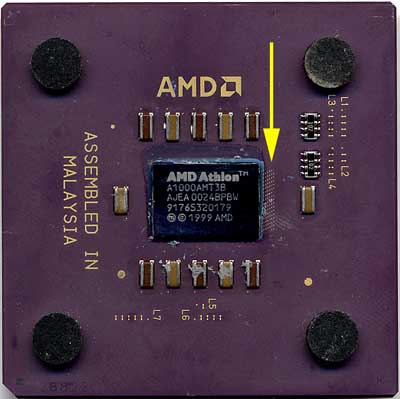
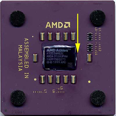
The Thunderbird core itself does have a smaller pattern of dots to its right, which originally led us to believe that a future version of the Athlon could have a larger L2 cache. AMD's roadmap at the time confirmed this with a processor that carried the codename Mustang, a larger cache version of the Athlon. Since then however AMD has cancelled the Mustang, and if you'll take a look at the new 1.33GHz part we have below, you'll see that the pattern of dots has disappeared as well.
"old" Athlon 1.1GHz
"new" Athlon 1.33GHz
It looks like the Athlon is not going to get any more than 256KB of L2 cache until the next die-shrink, which will be to a 0.13-micron process in the first half of 2002.


1 Comments
View All Comments
youcanyouwill - Sunday, January 5, 2020 - link
Thanks for sharing. https://www.carngo.com/car-rental/south-africa-nel...