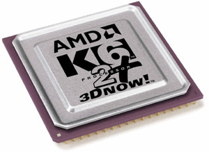
Super7 Upgrade Guide: The K6-2+ and K6-3+ Processors
by Matthew Witheiler on January 24, 2001 1:16 AM EST- Posted in
- CPUs
The Plus Means Better
In early 1999, AMD knew that both the aging K6-2 and K6-3 processors in their original forms needed some changes in order to enter more competitive markets and remain big sellers. In order to keep the Super7 alive, AMD had to make some changes to the K6 processor line in order to reinvigorate it. The approach taken was an interesting one. As the name suggests, the + series processors are closely related to their initial K6-2 and K6-3 brothers. The changes made to the processors turned out to be more than just a rehash of the old K6-2 and K6-3 cores and less than a completely new processor. Thus, the birth of the K6-2+ and K6-3+.
 The common alteration in the + line processors lies in the manufacturing process. Both the K6-2+ and the K6-3+ are manufactured on a 0.18 micron process, as opposed to the original K6-2 and K6-3's 0.25 micron process. The process shrink down to 0.18 micron resulted in a few benefits. First off, the smaller manufacturing process resulted in the ability to produce higher speed K6-2 and K6-3 based processors. By shrinking the process, less heat is produced at higher clock speeds. Since heat decreases the operational range of the transistors inside a processor, shrinking the process allows higher operational frequencies to be reached before encountering heat problems. This allowed AMD to ramp up clock speed with much greater ease, if needed. In the case of the K6-3+, the 0.18 micron process allowed the processor to hit 550 MHz, whereas the old 0.25 micron K6-3 only hit 450 MHz. With the K6-2+, however, AMD choose to limit the K6-2+ to the same speed as the original K6-2: up to 550 MHz.
The second thing that the smaller process allowed for is lower cost chips. Since shrinking the manufacturing process reduces the die size of a chip, less silicon was necessary to produce the + series processors. This allowed AMD to be even more aggressive in pricing, and area where they continue to stand out today.
It is with the manufacturing process shrink that the similarities between the K6-2+ and the K6-3+ end. From this point on, AMD decided to only change the K6-2+ from its original form, leaving the K6-3+ simply a regular K6-3 produced on a smaller fab. So what other alterations did the K6-2 get to transform it into the K6-2+ that we know today?
The answer is L2 cache, something that the original K6-2 had none of. In order to further distinguish the K6-2+ from the initial K6-2 incarnation, the K6-2+ gained an additional 128KB of L2 cache, upgrading from the original K6-2's 0KB of cache.
Previously, the K6-2 struggled with the lack of on-die cache, relying on the 66 - 100 MHz bus speed to carry data to and from external cache located on a motherboard. Not only did this hinder performance, it also inflated the cost of Super7 motherboards, as all high performing board were forced to include some sort of L2 cache on the motherboard. In fact, some manufacturers actually went as far as placing fake cache chips on boards, resulting in quite a bit of confusion and anger when consumers realized they had been had. While the K6-2 struggled with this problem, the K6-3 did not, as it already had 256KB of integrated L2 cache.
The transition to the 0.18 micron process provided a prime opportunity for AMD to include L2 cache on the K6-2 core. The die shrink provided the opportunity to include more items on the chip without increasing cost, hence the addition of the cache blocks. However, in order to still keep a distinction between the K6-3+ and the K6-2+, AMD chose to only put 128KB of on-die cache on the K6-2+ core. So, while the K6-3 only gained a die shrink in the K6-3+ version, the K6-2+ gained speed as well over its older brother.
All these changes may seem like a very intuitive plan for extending the longevity of Super7 based systems, but AMD had a different idea. Rather than place the K6-2+ and K6-3+ processors in the desktop market, where AMD was already struggling to get Athlon sales on their feet, the new processors were placed in a market were all the changes made sense: the notebook market.
The switch to the 0.18 micron process meant that the + series processors consumed much less power than their 0.25 micron counterparts. In mobile world, low power means big bucks, as it is power consumption that seems to be the Achilles heal for notebook manufacturers. With the new K6-2+ running off of a 1.4 - 2.0 volt socket and consuming 20 watts max, it had quite an advantage in the mobile arena over the original K6-2 which ran off of 2.2 - 2.8 volts and consumed 29 watts max. In a similar manner, the K6-3+ consumed a max of 23 watts and runs on the same 1.4 - 2.0 volt socket.
In addition, AMD decided to incorporate a new technology into the + series processors. Dubbed PowerNow, the new technology promised to revolutionize the way notebook computers use power. Described in detail in our PowerNow evaluation, the technology allowed the + series processors to dynamically change clock speed, making AMD even more poised to take a good amount of the mobile market.
So, while the K6-2+ and K6-3+ could potential increase speed in many Super7 desktop systems, AMD sold the processors only to OEMs with the intentions of using them in notebooks. But we can overcome that, can't we?


1 Comments
View All Comments
Leper Messiah - Tuesday, November 21, 2006 - link
^_^