The Intel SSD DC S3700 (200GB) Review
by Anand Lal Shimpi on November 9, 2012 8:01 AM EST- Posted in
- Cloud Computing
- Storage
- IT Computing
- SSDs
- Intel
Inside the Drive
I already went over the S3700's underlying architecture, including the shift from a B-tree indirection table to a direct mapped flat indirection table which helped enable this increase in performance consistency. I'll point you at that article for more details as to what's going on underneath the hood. For high level drive details, the excerpts below should give you most of what you need.
The S3700 comes in four capacities (100, 200, 400 and 800GB) and two form factors (2.5" and 1.8"). The 1.8" version is only available at 200GB and 400GB capacities. Intel sees market potential for a 1.8" enterprise SSD thanks to the increasing popularity of blade and micro servers. The new controller supports 8 NAND channels, down from 10 in the previous design as Intel had difficulty hitting customer requested capacity points at the highest performance while populating all 10 channels. 6Gbps SATA and AES-256 are both supported by the new controller.
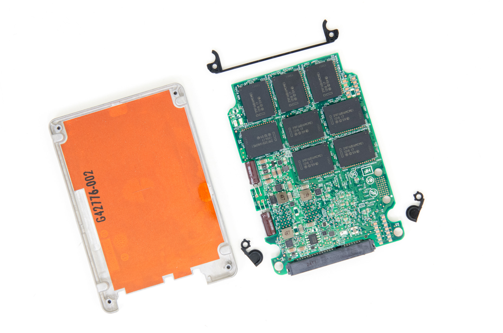
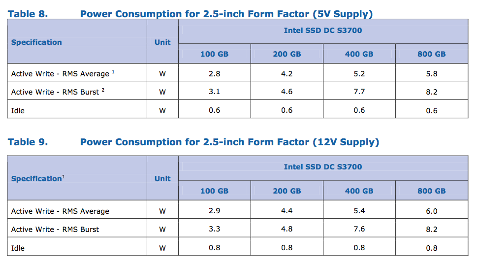
The S3700's chassis is 7.5mm thick and held together by four screws. The PCB isn't screwed in to the chassis instead Intel uses three plastic spacers to keep the board in place once the drive is put together. Along one edge of the drive Intel uses two 35V 47µF capacitors, enough to allow the controller to commit any data (and most non-data) to NAND in the event of a power failure. The capacitors in the S3700 are periodically tested by the controller. In the event that they fail, the controller disables all write buffering and throws a SMART error flag. Intel moved away from surface mount capacitors with the S3700 to reduce PCB real estate, which as you can see is very limited on the 2.5" drive. The S3700 supports operation on either 12V, 5V or both power rails - a first for Intel. Power consumption is rated at up to 6W under active load (peak power consumption can hit 8.2W), which is quite high and will keep the S3700 from being a good fit for a notebook.
The S3700 is a replacement to the Intel SSD 710 (the 710 will be EOLed sometime next year), and thus uses Intel's 25nm HET-MLC (High Endurance Technology) NAND. The S3700 is rated for full 10 drive writes per day (4KB random writes) for 5 years.
| Intel SSD DC S3700 Endurance (4KB Random Writes, 100% LBA) | ||||||
| 100GB | 200GB | 400GB | 800GB | |||
| Rated Endurance | 10DW x 5 years | 10DW x 5 years | 10DW x 5 years | 10DW x 5 years | ||
| Endurance in PB | 1.825 PB | 3.65 PB | 7.3 PB | 14.6 PB | ||
That's the worst case endurance on the drive, if your workload isn't purely random you can expect even more writes out of the S3700 (around 2x that for a sequential workload). Intel sent us a 200GB sample which comes equipped with 264GB of 25nm Intel HET-MLC NAND. Formatted capacity of the drive is 186GB in Windows, giving you a total of 78GB (78GiB technically) of spare area for wear leveling, block recycling, redundancy and bad block replacement. Note that the percent of overprovisioning on the S3700 is tangibly less than on the 710:
| Intel HET-MLC SSD Overprovisioning Comparison | ||||||
| Advertised Capacity | Total NAND on-board | Formatted Capacity in Windows | MSRP | |||
| Intel SSD 710 | 200GB | 320GB | 186GB | $800 | ||
| Intel SSD DC S3700 | 200GB | 264GB | 186GB | $470 | ||
Intel is able to guarantee longer endurance on the S3700 compared to the 710, with less spare area and built using the same 25nm HET-MLC NAND technology. The key difference here is the maturity of the process and firmware/controller. Both have improved to the point where Intel is able to do more with less.
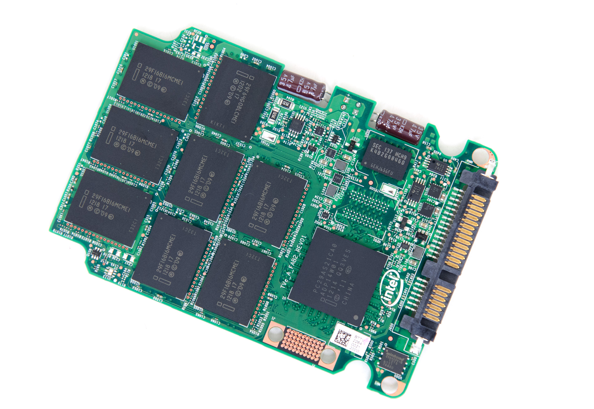
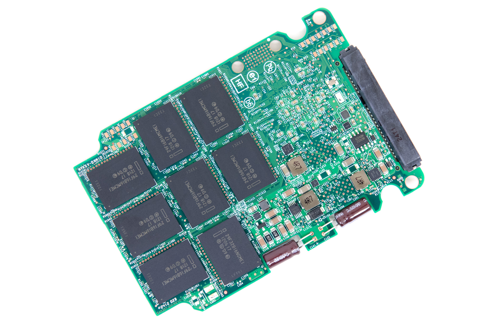
Because of the odd amount of NAND on board, there are 14 x 16GB, 1 x 32GB and 1 x 8GB NAND packages on this 200GB PCB. Each package uses between 1 and 4 8GB NAND die. Note that this is Intel's first SSD to use BGA mounted NAND devices. The controller itself is also BGA mounted, the underfill from previous generations is gone. The 8-channel controller is paired with 256MB of DDR3-1333 DRAM (the second pad is for a second DRAM used for the 800GB drive to reach 1GB of total DRAM capacity). Intel does error correction on all memories (NAND, SRAM and DRAM) in the S3700.
Pricing is much more reasonable than the Intel SSD 710. While the 710 debuted at around $6.30/GB, the Intel SSD DC S3700 is priced at $2.35/GB. It's still more expensive than a consumer drive, but the S3700 launches at the most affordable cost per GB of any Intel enterprise SSD. A non-HET version would likely be well into affordable territory for high-end desktop users. The S3700 is sampling to customers now, however widespread availability won't be here until the end of the year/beginning of Q1 2013.
| Intel SSD DC S3700 Pricing (MSRP) | ||||||
| 100GB | 200GB | 400GB | 800GB | |||
| Price | $235 | $470 | $940 | $1880 | ||
The S7300's performance is much greater than any previous generation Intel enterprise SATA SSD:
| Enterprise SSD Comparison | ||||||
| Intel SSD DC S3700 | Intel SSD 710 | Intel X25-E | Intel SSD 320 | |||
| Capacities | 100 / 200 / 400 / 800GB | 100 / 200 / 300GB | 32 / 64GB | 80 / 120 / 160 / 300 / 600GB | ||
| NAND | 25nm HET MLC | 25nm HET MLC | 50nm SLC | 25nm MLC | ||
| Max Sequential Performance (Reads/Writes) | 500 / 460 MBps | 270 / 210 MBps | 250 / 170 MBps | 270 / 220 MBps | ||
| Max Random Performance (Reads/Writes) | 76K / 36K | 38.5K / 2.7K IOPS | 35K / 3.3K IOPS | 39.5K / 600 IOPS | ||
| Endurance (Max Data Written) | 1.83 - 14.6PB | 500TB - 1.5PB | 1 - 2PB | 5 - 60TB | ||
| Encryption | AES-256 | AES-128 | - | AES-128 | ||
| Power Safe Write Cache | Y | Y | N | Y | ||
Intel is also promising performance consistency with its S3700. At steady state Intel claims the S3700 won't vary its IOPS by more than 10 - 15% for the life of the drive. Most capacities won't see more than a 10% variance in IO latency (or performance) at steady state. Intel has never offered this sort of a guarantee before because its drives would vary quite a bit in terms of IO latency.
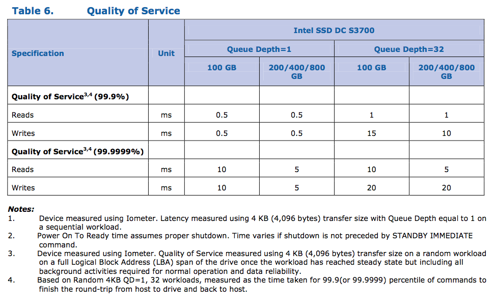
Intel also claims to be able to service 99.9% of all 4KB random IOs (QD1) in less than 500µs:
The lower latency operation is possible through the use of a flat indirection table (and some really well done firmware) in the new controller. What happens now is there's a giant array with each location in the array mapped to a specific portion of NAND. The array isn't dynamically created and, since it's a 1:1 mapping, searches, inserts and updates are all very fast. The other benefit of being 1:1 mapped with physical NAND is that there's no need to defragment the table, which immediately cuts down the amount of work the controller has to do. Drives based on this new controller only have to keep the NAND defragmented (the old controller needed to defragment both logical and physical space).
The downside to all of this is the DRAM area required by the new flat indirection table. The old binary tree was very space efficient, while the new array is just huge. It requires a large amount of DRAM depending on the capacity of the drive. In its largest implementation (800GB), Intel needs a full 1GB of DRAM to store the indirection table. By my calculations, the table itself should require roughly 100MB of DRAM per 100GB of storage space on the drive itself. There's a bit of space left over after you account for the new indirection table. That area is reserved for a cache of the controller's firmware so it doesn't have to read from slow flash to access it.
Once again, there's no user data stored in the external DRAM. The indirection table itself is physically stored in NAND (just cached in DRAM), and there are two large capacitors on-board to push any updates to non-volatile storage in the event of power loss.
It sounds like a simple change, but building this new architecture took quite a bit of work. With a drive in hand, we can put Intel's claims to the test. And there's one obvious place to start...


30 Comments
View All Comments
RealNinja - Tuesday, November 6, 2012 - link
Looks like a nice enterprise drive. Will be interesting to see how reliable the new controller is in the "real world."For my consumer money...still gotta go with Samsung right now.
twtech - Tuesday, November 6, 2012 - link
Looks like a nice workstation drive as well. With that kind of write endurance, it should be able to handle daily multi-gigabyte content syncs.futrtrubl - Saturday, November 10, 2012 - link
Umm, with that write endurance it should be able to handle daily multi-TERAbyte syncs, seeing as it is rated at 10x capacity/day for 5 years.CeriseCogburn - Wednesday, January 2, 2013 - link
I watched the interview, and saw all 3 of the braggarts spew their personal fantasies and pride talk, then came here to take a look, and I'm not impressed.I do wonder how people do that.
DanNeely - Tuesday, November 6, 2012 - link
"I had to pull Micron's P400e out of this graph because it's worst case latency was too high to be used without a logarithmic scale. "Could you add the value to the text then?
crimson117 - Tuesday, November 6, 2012 - link
Move away from NAND - to what?stmok - Tuesday, November 6, 2012 - link
...To Phase Change Memory (PCM).DanNeely - Tuesday, November 6, 2012 - link
Everything old (CDRW) is new again!martixy - Friday, November 9, 2012 - link
Right... so we got that covered. :)Now we're eagerly awaiting the next milestone towards the tech singularity.
Memristor - Wednesday, November 7, 2012 - link
To Memristor