Creative Labs Annihilator2 Ultra 64MB GeForce2 Ultra
by Anand Lal Shimpi on October 26, 2000 1:25 AM EST- Posted in
- GPUs
The Card
Once again, just as we saw with ELSA’s GeForce2 Ultra solution, the Annihilator2 Ultra is based upon NVIDIA’s reference design. The idea of video card manufacturers using a video chipset manufacturer’s reference design in an actual production card is pretty new, since the reference designs of yesterday left quite a bit to desire. For the end user it’s hard to tell the difference, but for the video card manufacturer the lack of detail present in many of those old reference designs made following them useless. And thus we saw many variations on cards by different manufacturers that all featured the same chipset.
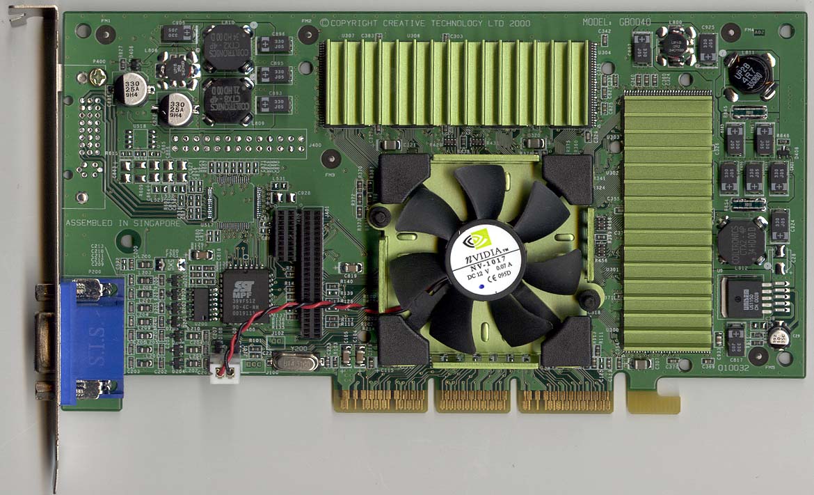
Things have since changed and it’s now very commonplace for video card manufacturers to follow NVIDIA’s design unless they are implementing some features that aren’t provided for in the reference design. It’s much easier this way for the manufacturer to crank out a card based on a newly released chipset as it saves a lot of the time that would otherwise be devoted to creating a new design from scratch. Which makes Creative Labs’ decision pretty sensible.
However, at least according to Creative Labs, the card design process isn’t as simple as following the reference design and producing cards. Instead Creative Labs implements a rigorous testing procedure in which they put NVIDIA’s reference design to the test just to make sure that the design is sufficient for their needs. While in most cases this level of quality control isn’t necessary, for Creative Labs, it’s most definitely necessary when you’re dealing with the extremely large volume of cards that they ship. You won’t see any reliability issues with these cards as you would with some of the smaller manufacturers that don’t implement such extensive testing methods, however the likelihood that you’d run into such a problem with any card based on NVIDIA’s reference design is very low.
 The
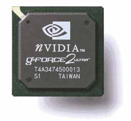
heart of the Annihilator2 Ultra is its 0.18-micron GeForce2 Ultra core which
is clocked at 250MHz, a full 25% higher than the regular GeForce2 GTS. In order
to maintain a GeForce2 Ultra production line, NVIDIA only selects the highest
quality GeForce2 parts to be labeled as an Ultra. As we saw in our July 2000
GeForce2 GTS Roundup, only half of the cards hit a 250MHz core clock, and none
of them managed to go even 5MHz higher. Most GeForce2 GTS parts seem to be
happy in the 225 – 235MHz range with regular cooling, but this means that NVIDIA
has to work fairly hard to get an Ultra part out of the bin. Of course, as
time goes on, yields do improve so there are most likely more GeForce2 GTS’
hitting 250MHz now than there were last July, but you get the point; in order
to hit 250MHz, much more than just increasing the clock on the chip is necessary.
The
heart of the Annihilator2 Ultra is its 0.18-micron GeForce2 Ultra core which
is clocked at 250MHz, a full 25% higher than the regular GeForce2 GTS. In order
to maintain a GeForce2 Ultra production line, NVIDIA only selects the highest
quality GeForce2 parts to be labeled as an Ultra. As we saw in our July 2000
GeForce2 GTS Roundup, only half of the cards hit a 250MHz core clock, and none
of them managed to go even 5MHz higher. Most GeForce2 GTS parts seem to be
happy in the 225 – 235MHz range with regular cooling, but this means that NVIDIA
has to work fairly hard to get an Ultra part out of the bin. Of course, as
time goes on, yields do improve so there are most likely more GeForce2 GTS’
hitting 250MHz now than there were last July, but you get the point; in order
to hit 250MHz, much more than just increasing the clock on the chip is necessary.
Part of those heightened requirements is the use of a larger heatsink with a more powerful fan which allows to keep the chip running cool and reliable. From what we’ve seen, most GeForce2 GTS based cards run at about 124F (temperature taken from the back of the PCB directly behind the core), and as you can probably imagine, using conventional cooling methods a 25% higher clocked chip would definitely produce quite a bit more heat. The solution was obvious, use a larger heatsink.


0 Comments
View All Comments