AMD's K6-2+ in Notebooks - Evaluating Performance with PowerNow
by Anand Lal Shimpi on September 12, 2000 7:06 PM EST- Posted in
- Laptops
Super7 Lives: AMD's K6-2+
 At
last year's Comdex, surrounded by Athlons that were hitting impressively high
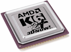
clock speeds and promises of a very bright future for AMD, we were introduced
to an interesting little processor, the K6-2+.
At
last year's Comdex, surrounded by Athlons that were hitting impressively high
clock speeds and promises of a very bright future for AMD, we were introduced
to an interesting little processor, the K6-2+.
With the Athlon and its forthcoming Spitfire (now known as the Duron) successor primed to take over AMD's entire processor line, the future of the Super7 platform that had kept AMD alive over the year and a half prior to the Athlon's entrance was very uncertain.
Even AMD had seemed to abandon the Super7 platform, not without good reason. The Athlon was destined to become just as affordable as the older Super7 processors were, without the headaches and the poor FPU performance that characterized its predecessors.
In spite of this clear move away from the Socket that had carried AMD for quite a while, the company had on display, in one corner of their suite, a brand new Super7 processor. However the K6-2+ wasn't running in the same old desktop Super7 boards we were used to seeing, rather it was in a notebook.
With the first Athlons with power requirements in the 50 - 54W range (0.25-micron K7 core), there was no way that AMD could maintain a successful mobile CPU line based on the Athlon core in its current form. Even using the 0.18-micron Athlons wasn't a possibility because their power consumption was still in the 30 - 48W range.
In order to fill this void in their product line, they took their previous generation K6-III, which was fairly successful in areas that did not require heavy floating point computations, and changed it around a bit in order to better suit the needs of the mobile market.
If you'll recall, upon its introduction, the 0.25-micron K6-III was essentially based on the K6-2 core with the addition of a full-speed 256KB L2 cache on-die. This would later be a part of what AMD called their TriLevel Cache design which consisted of the on-die L1 and L2 caches and an optional on-board L3 cache (up to 1MB).
 The
K6-2+ makes use of a smaller 0.18-micron fabrication process, thus decreasing
power consumption and heat production as well as increasing the number of chips
AMD could produce per wafer at their plants. The addition of the '+' to the
end of the K6-2 name indicates the use of AMD's 0.18-micron fabrication process,
the same holds true for the K6-III+.
The
K6-2+ makes use of a smaller 0.18-micron fabrication process, thus decreasing
power consumption and heat production as well as increasing the number of chips
AMD could produce per wafer at their plants. The addition of the '+' to the
end of the K6-2 name indicates the use of AMD's 0.18-micron fabrication process,
the same holds true for the K6-III+.
All '+' chips including the K6-2+ feature the same Enhanced 3DNow! instructions that were originally introduced with the Athlon processors last August.
The K6-2+'s TriLevel cache design deviates from the original K6-III's implementation in that it features a 128KB 4-way set associative on-die L2 cache, rather than a 256KB cache. The CPU still features the same 64KB 2-way set associative L1 cache as its predecessors, and still allows for up to a 1MB external, on-board L3 cache. However it is highly unlikely that you'll see any mobile configurations with any L3 cache, much less 1MB, simply because of space constraints.
The K6-2+ still operates on the same 100MHz FSB and 100MHz memory bus, but thanks to the processor's on-die L2 cache, the 100MHz FSB isn't the limitation it used to be with the first desktop K6-2s.
However, quite possibly the most important feature of the K6-2+ (and the K6-III+) is its support for a little feature AMD likes to call PowerNow! In fact, the K6-2+'s PowerNow! support is what makes the processor an attractive option for mobile users.


1 Comments
View All Comments
Dr AB - Saturday, May 9, 2020 - link
PowerNow! - a very clever idea back then to dynamically adjust cpu freq & VID output. The same idea still exists in today's day and age. No wonder where did intel took the inspiration from.