The Card
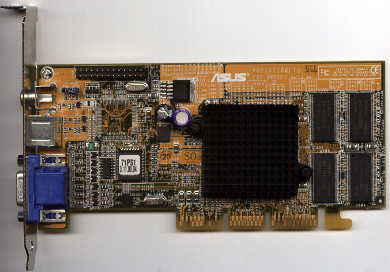
Following the path we expect more and more manufacturers to take, ASUS has chose to vary from the GeForce2 MX's reference design to minimize PCB space and maximize efficiency. In fact, ASUS has changed a few items on the V7100, opting to use a customized design, a strategy which we have seen ASUS use many times in the past. More on what exactly ASUS changed in a minute, but for now note the small PCB space that the V7100 takes up, making it look very similar to the Guillemot/Hercules GeForce2 MX based product..
The rather cool .18 micron GeForce2 MX GPU is cooled via a standard 4.5 x 4.5 cm heatsink that is appropriately bonded to the MX's surface via thermal grease. This automatically gives the V7100 quite an advantage over many other GeForce2 MX based cards out there that lack any form of cooling. Although this passive form of cooling may not work as well as a fan and heatsink combination, it is still quite a step above some of the other naked products we have seen. In fact, this heatsink seems to ad more than one selling point to the V7100, because as a result of the cooling employed ASUS was able to bring the V7100 to market with a core speed of 180 MHz, 5 MHz over the suggested NVIDIA clock speed. We are unsure if it is just our test sample that came with the overclocked core or if every V7100 sold will come with it but regardless it is almost certain that every V7100 sold will be able to hit this speed.
On the downside, the method of bonding the GPU to the heatsink was good but the pins used to hold it in place were not. The pins used to hold the heatsink to the chip surface are a bit different than the clips we have seen in the past, which proved to be a problem, as the functionality of these clips is not as good as what we have seen in the standard clips. The clips popped out of the mounting holes rather easily, leaving our heatsink only half attached quite a few times during testing. This problem seems to be a result of the thinner plastic used on this clips. Normally this will not be a problem, as the video card will stay stationary for the majority of its life. Just be careful when putting the card in and make sure that both clips are fully inserted.
As we mentioned before, the V7100 comes in two different memory configurations, both a 16MB and a 32MB one. Our test sample was a 32MB card, an option that we suspect that the vast majority of people will choose in order to gain the most speed from the GeForce2 MX chip. Our configuration of the card came with 6ns SDR Hyundai SDRAM chips. Although these chips may not be as fast as the 5.5ns version we have heard of on the Guillemot/Hercules based card, they are still within spec, a problem we encountered with the VisionTek GeForce2 MX. In addition, we have heard of the Guillemot/Hercules cards coming with everything from the 5.5ns RAM to 7ns memory, meaning that memory speed and type may not be certain any more. In the case of our V7100, the memory clock on our card was actually pushed up to 171 MHz, once again exceeding NVIDIA's suggested speed by 5 MHz. This also, coincidentally, exceeded Hyundai's specification for the RAM chips by 5 MHz as well. Once again, we are not certain if cards will come to market with these speeds, but it should not be a problem getting the vast majority to achieve this modest overclock.
 Ok,
now back to what ASUS has changed on the V7100 that makes it look a bit different
than other MX based video cards. As we mentioned before, our model of the V7100
was branded the V7100/T, making it the TV-out version of the V7100. You may
notice that there is no daughter board controlling the video-out features of
the card. In fact, there are not even pin headers to allow for the addition
of an add-on board. Rather than take the path that every other MX based video
card manufacturer has taken since the release of the product, ASUS decided to
ditch the whole daughter board idea and place the TV-out components of the card
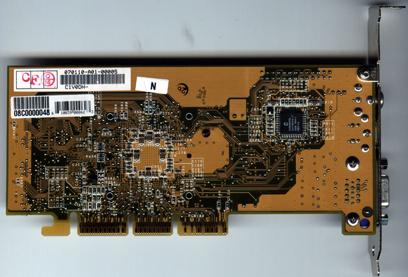
on card. This required some slight modification of the GeForce2 MX reference
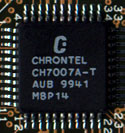
design, with the placement of a Chrontel CH7007A chip on the back of the card.
If you recall from our previous ASUS reviews, ASUS has been using the Chrontel
chip over the commonly found Brooktree 869 chip found on almost every other
NVIDIA based card with TV-out. This proved to be a wise decision, as the Chrontel
chip seems to have just as good, if not better video output than the Brooktree
chip.
Ok,
now back to what ASUS has changed on the V7100 that makes it look a bit different
than other MX based video cards. As we mentioned before, our model of the V7100
was branded the V7100/T, making it the TV-out version of the V7100. You may
notice that there is no daughter board controlling the video-out features of
the card. In fact, there are not even pin headers to allow for the addition
of an add-on board. Rather than take the path that every other MX based video
card manufacturer has taken since the release of the product, ASUS decided to
ditch the whole daughter board idea and place the TV-out components of the card
on card. This required some slight modification of the GeForce2 MX reference
design, with the placement of a Chrontel CH7007A chip on the back of the card.
If you recall from our previous ASUS reviews, ASUS has been using the Chrontel
chip over the commonly found Brooktree 869 chip found on almost every other
NVIDIA based card with TV-out. This proved to be a wise decision, as the Chrontel
chip seems to have just as good, if not better video output than the Brooktree
chip.
 In
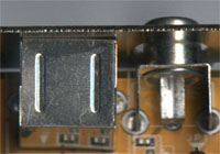
addition to switching the the video-out decoder to the back of the card, ASUS
also had to place the S-video and composite out connectors on the board itself,
as opposed to on the daughter card that other GeForce2s use. Accomplishing this
feat by placing the connectors where the DVI or Dual-Head VGA ports would be,
ASUS managed to fit both connectors on the card. The incorporation of the connectors
on the card is great for home entertainment users, as the dual-head abilities
of the card allows it to display two applications on different screens, for
example one could watch a DVD movie on a nearby TV while also surfing the web
on the monitor.
In
addition to switching the the video-out decoder to the back of the card, ASUS
also had to place the S-video and composite out connectors on the board itself,
as opposed to on the daughter card that other GeForce2s use. Accomplishing this
feat by placing the connectors where the DVI or Dual-Head VGA ports would be,
ASUS managed to fit both connectors on the card. The incorporation of the connectors
on the card is great for home entertainment users, as the dual-head abilities
of the card allows it to display two applications on different screens, for
example one could watch a DVD movie on a nearby TV while also surfing the web
on the monitor.
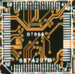 On
an interesting note, the V7100 also has a blank space on the board for the placement
of the Brooktree 869 chip that we spoke of earlier. We are not quite sure why
ASUS would choose to include a place for this chip on their reference design
board (as the Chrontel chip on the back accomplishes the exact same thing),
however it is possible that they will switch chips later in production.
On
an interesting note, the V7100 also has a blank space on the board for the placement
of the Brooktree 869 chip that we spoke of earlier. We are not quite sure why
ASUS would choose to include a place for this chip on their reference design
board (as the Chrontel chip on the back accomplishes the exact same thing),
however it is possible that they will switch chips later in production.


0 Comments
View All Comments