VIA Apollo KX133 Athlon Chipset - Part 1
by Anand Lal Shimpi on February 7, 2000 11:51 PM EST- Posted in
- CPUs
The KX133 chipset actually isn’t very new. In fact, most of the technology that went into the design of the KX133 has been around for quite some time. Originally, the KX133 was supposed to be ready and shipping by the launch of the Athlon last August, but, unfortunately, according to VIA, that was delayed for a number of reasons, including the fact that they wanted to work closer with motherboard manufacturers on their implementations to get them right the first time.
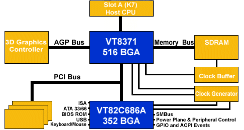
The KX133 itself takes advantage of a number of borrowed features from other VIA products. The chipset itself, in the usual VIA style, is divided into two parts, a 516-pin North Bridge, the VT8371, and a 352-pin South Bridge, the VT82C686A that we’re already quite familiar with.
VIA still hasn’t accepted an approach more like Intel’s Accelerated Hub Architecture, which, through the use of an all-purpose-bus, is capable of transferring data at 266MB/s. VIA’s KX133, like all previous VIA chipset, relies on the PCI bus to connect the North Bridge to the South Bridge thus offering a peak theoretical bandwidth figure of 133MB/s. This bottleneck, although still not very apparent with Athlon systems (the AMD 750 features the same “bottleneck” and performs just fine) is something that VIA will have to consider in future chipset implementations, they just chose not to start with the KX133.


0 Comments
View All Comments