Intel & Micron Announce 25nm NAND Flash Production, SSDs to get Bigger/Cheaper in Q4
by Anand Lal Shimpi on January 30, 2010 12:00 AM EST- Posted in
- Storage
I wasn’t supposed to be able to tell you about this until Monday, but it looks like the news leaked early so IMFT gave us the green light.
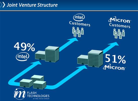
Intel and Micron jointly formed IMFT (Intel-Micron Flash Technologies), LLC back in 2006. The two companies share production from the venture. Intel gets 49% of IMFT’s flash production and Micron gets 51%.
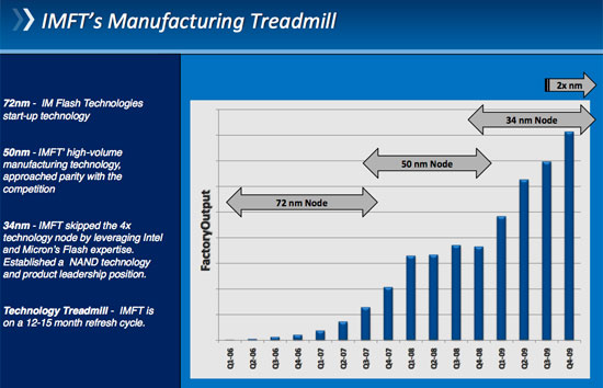
In the usual Intel tradition, IMFT aggressively scales process technology to be competitive. The company started manufacturing at 72nm, spent 2008 at 50nm and just last year scaled down to 34nm. The latter is what found its way into Intel’s X25-M G2 as well as Micron’s soon-to-be released RealSSD C300.
Today IMFT is announcing that it has begun sampling 2-bits-per-cell MLC NAND flash manufactured using 25nm transistors. The company believed it had a 6 month head start over the competition in 34nm, and now believes that with 25nm NAND it’s roughly a year ahead of anyone else.
Volume production will happen sometime in Q2, with products shipping before the end of the year. In my last SSD article I mentioned that Intel’s 3rd generation X25-M would be shipping in Q4 at 160GB, 320GB and 600GB. These drives will use IMFT’s new 25nm flash.
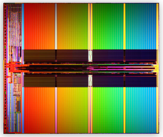
The first 25nm product is an 8GB (64Gbit) 2-bits-per-cell MLC NAND flash. A single 8GB die built on IMFT’s 25nm process has a die size of 167mm2. Immersion lithography is apparently necessary to produce these 25nm NAND devices, but the extent is unclear. This is technically Intel’s first device that requires immersion lithography to manufacture.
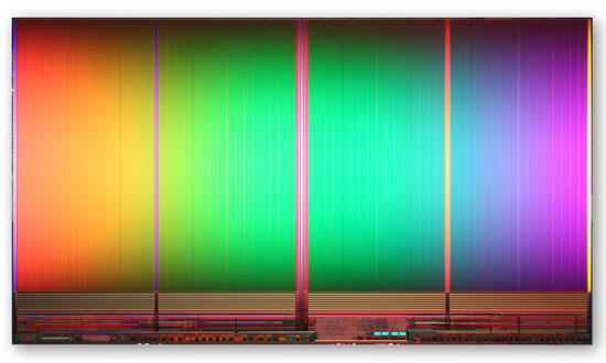
25nm IMFT 2-bit MLC NAND Flash, 8GB, 167mm2
The 34nm flagship was a 4GB (32Gbit) 2-bits-per-cell MLC NAND device with a die size of 172mm2. At 25nm you basically get twice the capacity at the same die size, which should translate into twice the SSD capacity at the same price as a 34nm drive today.
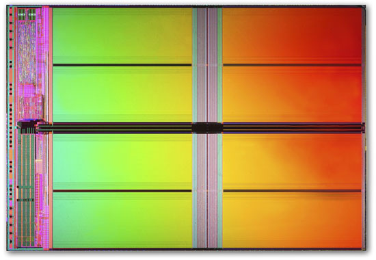
34nm IMFT2-bit MLC NAND Flash, 4GB, 172mm2
Obviously supply and demand economics play their roles here. We may not see the sort of aggressive pricing we want to on 25nm X25-M drives if demand remains as high as it has been for the 34nm G2s.
Last year IMFT announced plans to deliver a 3-bit-per-cell 34nm MLC NAND flash. Today's announcement pretty much negates the need to bring those devices to market. Although at some point we'll probably see 3-bit-per-cell at 25nm. At this point 3-bit-per-cell MLC flash is only suitable for cheaper or low cycle devices like USB sticks. In a SSD the performance and reliability tradeoffs just aren't worth it.
34nm IMFT 3-bit MLC NAND Flash, 4GB, 126mm2
The 25nm IMFT NAND devices support ONFi 2.2, meaning the interface speed can reach a maximum of 200MB/s.
The other major change to the 25nm NAND is an increase in the page size. At 50nm and 34nm, IMFT’s page size was 4KB. At 25nm on the 8GB device the page size is now 8KB. Block size has also gone up from 128 pages to 256 pages. This will obviously have performance implications and require some firmware reorganization, but given that Intel has known this was coming for some time now I would expect that its 3rd generation drives will be optimized for 25nm.
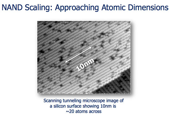
IMFT believes there’s still hope for scaling flash devices even further. It's ridiculous to think about how small these transistors are getting. As we approach single-digit-nm dimensions we can start counting atoms when we look at these transistors:
Right now IMFT is on a 12 - 15 month cycle, so we can expect the next process shrink to begin sampling in mid-2011, shipping in 2012.
If IMFT can ramp up production of 25nm NAND flash, 2012 may be the year of the first truly affordable mainstream SSDs.


39 Comments
View All Comments
kunedog - Thursday, February 18, 2010 - link
As of yesterday, Newegg has the OEM G2 X-25M 80GB for $220 shipped and the 160GB for $430 shipped:http://www.newegg.com/Product/Product.aspx?Item=N8...">http://www.newegg.com/Product/Product.aspx?Item=N8...
http://www.newegg.com/Product/Product.aspx?Item=N8...">http://www.newegg.com/Product/Product.aspx?Item=N8... (comes with a free USB enclosure)
This is the FIRST time they have been in stock for more than a day at anywhere near the retail prices that Anand predicted over SIX MONTHS ago:
http://www.anandtech.com/storage/showdoc.aspx?i=36...">http://www.anandtech.com/storage/showdoc.aspx?i=36...
Butch306 - Monday, February 1, 2010 - link
I'd be happier with an announcement that a firmware upgrade is available to fully implement TRIM on a Raid setup. As much as I'm always ready to upgrade to the biggest, latest and greatest; no TRIM support in Raid is a potential huge show stopper to upgrade from current Intel 34nm G2 SSDs on my annual next build. Which ever manufacturer comes out with a proper/equivalent solution to keep SSDs in multiple Raid configurations operating at their peak efficiency is going to get my money.jhh - Tuesday, February 2, 2010 - link
TRIM is a horribly implemented command in SATA drives, as TRIM is a synchronous command. All the read-ahead and write-behind operations block waiting for TRIM to finish. One proposal from the Linux community was to allocate blocks from a "already written" pool instead of using TRIM. This would allow the never-written area of the drive unwritten as long as possible.kensiko - Tuesday, February 2, 2010 - link
Yeah but this will prevent wear leveling system to do its work.For RAID with TRIM, on OCZ forum, someone pointed out the RAID capability of Win7 that would probably allow TRIM and RAID together. But, of course, software RAID isn't as good as hardware RAID.
AtwaterFS - Sunday, January 31, 2010 - link
since SSD's are the cause for a fatter SATA pipe...Xyn - Sunday, January 31, 2010 - link
So the 25nm process will be rolled out at all their plants? I was wondering what IM Flash Technologies was, since they built a new plant near my house.So I guess ~5nm will be the limit before you reach atomic levels, aye? Might be good news or bad news, I'm not sure.
jimhsu - Sunday, January 31, 2010 - link
Immersion lithography is only a stopgap solution because it relies on the greater index of refraction of water. Since we really don't have many fluids with an even larger index of refraction, I'm highly curious how low 2x and 1x nm will be attempted - double patterning? nanofabrication?jimhsu - Sunday, January 31, 2010 - link
Personally, I think true nanomachines (as in bottom-up assembly?) will appear at 11 nm or below, based on my rudimentary understanding of chip fabrication and reading on wikipedia. You simply can't make silicon much smaller than that.GullLars - Sunday, January 31, 2010 - link
With a 1,414x shrink between each full process node, you have 4 shrinks left after 25nm until you reach 5nm. With 15 months between each process node that gives 5 years... At that point you need to start 3D processes to scale further, or start using nano-technology.ONFI 2.2 specifies 200MB/s interface bandwidth max for each flash channel, you may have multiple ICs (packages), each with multiple dies, pr flash channel. It will essentially enable higher bandwidth at fewer channels, wich means lower controller design costs and less complexity. You also run into a push to larger page sizes and block sizes in order to scale the bandwidth effectively from a single IC. 4KB random read bandwidth will not take a huge hit (rather stay about the same as today), as partial page reads are easily done, it will however not scale from todays 32nm chips (pr channel).
Turas - Sunday, January 31, 2010 - link
I am wondering if the other memory vendors will have to do the same? Also what will the perf impact be as we are already dealing with filesystems designed for spinning disks? They have added trim/gc items but wondering if the whole filesystem is next thing to really need a overhaul.