P55 Overclocking Showdown - ASUS, Gigabyte, and EVGA at the OC Corral (Page 6 Updated)
by Rajinder Gill on November 6, 2009 12:00 PM EST- Posted in
- Motherboards
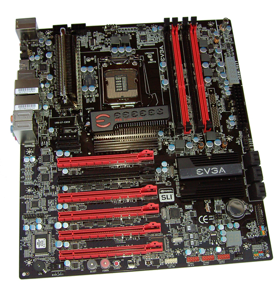
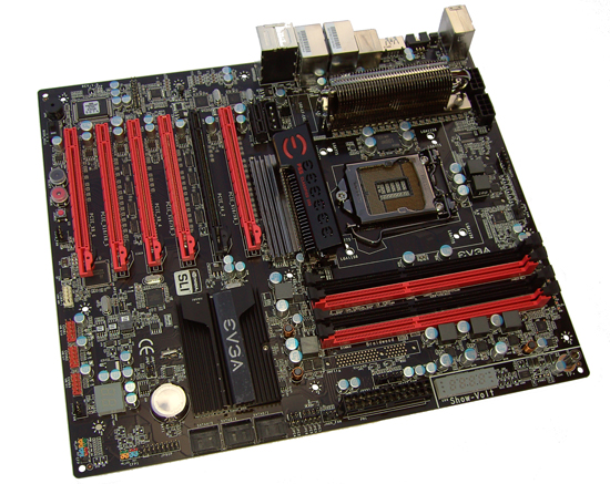
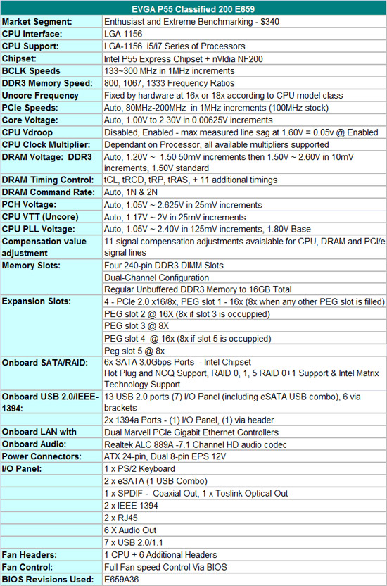
EVGA’s top end offering for P55 is overkill in every single way. Classified specs add a 10-phase Volterra PWM for CPU power, a lower inductance LOTES CPU socket, an onboard digital multi-meter, and an NF200 bridge chip that adds support for triple 16x SLI or CrossFire. Like the P55 FTW E657, version 2 of EVGA’s OCP (overclocking panel) is included giving more than a subtle hint at who this board is designed for.
Priced at $340 or so, this board is more about what EVGA can do than what they should have done for this platform. The existence of X58 fills this segment with a slew of multi-gpu capable boards on the robust and higher performance socket 1366 platform. Nevertheless, we’ve added overclocking results so those who are interested can see how this board fares against others when teamed with the same components and within the same test environment.
Like the E657 model, 7 onboard fan headers are provided with full speed control via BIOS. Due to the addition of the onboard digital multi meter the E659 is classed as E-ATX with dimensions of 304.8mm X 243.8mm (LXW). This might make things a little cramped in smaller PC cases, although we think that anyone choosing a board like this is either going to be someone running an open test bed for benchmarking purposes or is someone who uses a lavish full tower PC case.
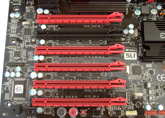
The presence of the NF200 brings a total of six 16x (mechanical) PCI/e slots and one PCI/e x1 slot to the E659. PCI/e X1 at the top, followed by the primary PEG slot running at 16x width in single GPU mode (8x when other PEG slots are occupied).For a full breakdown on lane allocation/link width check the specification table below.
No PCI slots are present on this board, which probably is not a big deal to the intended audience. Slot layout is flexible enough to cater for just about every type of configuration leaving ample upgrade room. We don’t have multi-card performance numbers at this time, although may update later if there is demand to do so.
Underneath the last PCI/e slot, we find power, reset and CMOS clear buttons. A 3 way slider switch is also provided allowing user selection of 3 separate BIOS IC’s. This allows flashing 3 different BIOS files, and also adds a good level of security in the instance of a corrupt BIOS flash. Two USB headers and a IEEE-1394a header are also placed along the bottom edge of the board.
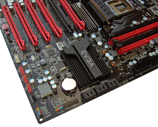
A hex post code display is placed in the lower right corner of the board and over to the left we find 3 BIOS IC’s, one of which is placed within a socket allowing removal if a swap out is required. The CFP1 connector is the EVGA OCP PCB panel connector which allows for on the fly changes 0.1V boost functions to CPU VCore and VTT as well as a post code reader and power, reset and CMOS clear buttons.
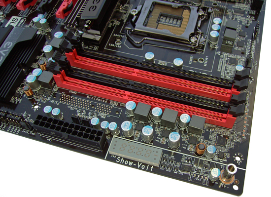
PCI/e disable and X-Cool jumpers are located underneath the DIMM slots. Memory power is supplied by a three phase controller supporting switching speeds up to 640KHz. A test lead is supplied to plug into the positive input socket of the onboard DMM. Test pads for all primary voltage rails are located above the DIMM slots.
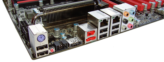
On the rear I/O panel we find 1 x PS2, 7 X USB (1 SATA combo), 1x S/PDIF, 1x Optical, 1 x 1394, 2x RJ45 LAN and 6 audio connectors. A push CMOS reset button is located between the PS2 and S/SPDIF connectors for easy CMOS clear events.
The E657 and E659 models share a practically identical BIOS (refer to screenshots on the E657 page). The only notable changes being the addition of voltage control for the added NF200 on the E659 model, together with an additional compensation adjustment for the CPU.


52 Comments
View All Comments
spacedude - Thursday, January 7, 2010 - link
Just wanted to comment that I just ordered a EVGA P55 SLI (NOT FTW) from newegg and received a foxconn socket...Though on the forums, the evga reps are insistent that there is no problem with their boards.... Who knows if I even have a revised socket........
ARGHHHHHHH
johnyfriend - Tuesday, November 17, 2009 - link
Saw recently a number of boards from asus and gigabyte with Usb3 and Sata 6gb support.Are you guys planning to include those boards in your upcoming p55 board reviews?groove420 - Saturday, November 21, 2009 - link
The new Gigabyte boards will be designated as "P55A-UD6" for example, along with a "333" designation on the box.The feature that caught my eye on these is that they have been refitted with a LOTES clamp instead of the Foxconn.
They remain fitted with a Foxconn socket apparently though.
Whether the fix for the "hot socket" was just a better clamp, or indeed the socket is a revision as well remains an unknown from what I've gathered.
johnyfriend - Tuesday, November 24, 2009 - link
Think they went with the more afordable way to change the clamps than the entire socket.got to wait and see if it pays out..incase those who are willing to buy decide to dump $$$$$$$$ in thatArbie - Monday, November 9, 2009 - link
"Be warned the results are geared more towards benchmarking fanatics and are not in any way indicative of your everyday web browsing PC needs... "Is this a benchmarking fanatics website? Or is it aimed at folks who want high-performance gear for day-in, day-out use? I am in the latter group, which is why I visit AnandTech practically every day. But I won't even bother clicking through a report like this.
In fact, probably only 0.1% of your readers are going to build on the edge (sub-zero cooling?), and there are plenty of websites for them. I'd rather see the same time and effort spent on something more relevant to the other 99.9%.
My opinion...
dingetje - Monday, November 9, 2009 - link
fail troll, stop whining or go to tomshardwarematthewfoley - Tuesday, November 10, 2009 - link
I happen to agree 100% - I am interested in the high-performance gear for day-in, day-out use idea.Anybody who wants Lynnfield for breaking OC benchmarks is wasting their time.
dia - Tuesday, November 10, 2009 - link
99% of the articles here are for regular users. This happens to be an article that is not for everyone. So what's the big deal if the minority audience occasionally gets a hearing every now and again? When I see articles like this going up every single week I might start to ask questions, but not before that.AstroGuardian - Wednesday, November 11, 2009 - link
Guys and gals,This article is 100% for everyone despite what other ppl say.
You are totally missing the point of this post. This post is not about manufacturers and main boards. This post is about P55!!!
I am sure everyone (including benchmark fanatic) would like to hear about P55's capabilities. This article says about P55's abilities and gives insight about possible scenarios when pushing the P55 to its limits.
So what do you want to say? Do you criticize this site or what? Not all of you are IT professionals. As a matter of fact so few of you are IT professionals. And as professionals you musk know as much as possible about your area of expertise. I would like to know everything Anandtech has to say about everything. That's the beauty of it
cyclo - Wednesday, November 11, 2009 - link
+1. I rarely overclock myself but I still am interested in what the capabilities of this CPU/chipset combo are. I like seeing systems pushed to their limits until weaknesses become apparent. Extreme overclocking in my opinion is like stress testing... if there is any weakness in a design overclocking can expose it. In this case it could be the Foxconn socket, the lesser number of pins on the CPU itself (compared to previous gen i7s), the interface, or all of the above.