NVIDIA's 1.4 Billion Transistor GPU: GT200 Arrives as the GeForce GTX 280 & 260
by Anand Lal Shimpi & Derek Wilson on June 16, 2008 9:00 AM EST- Posted in
- GPUs
One-Point-Four-Billion. That's transistors folks.
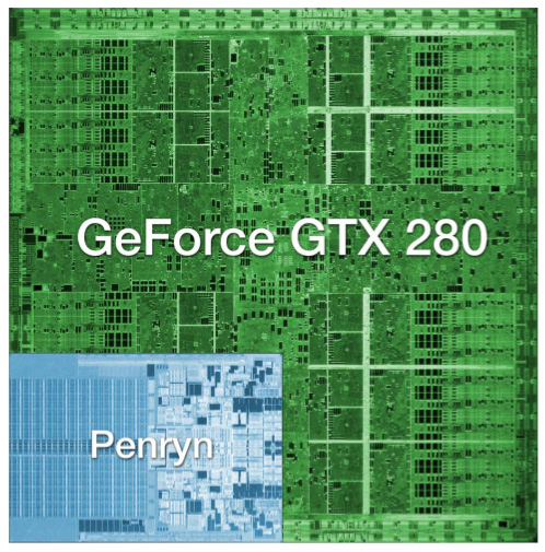
The chip is codenamed GT200 and it's the successor to NVIDIA's G80 and G92 families. Why the change in naming? The GT stands for "Graphics Tesla" and this is the second generation Graphics Tesla architecture, the first being the G80. The GT200 is launching today in two flavors, the die of the larger one is pictured below:
Um...yeah...we're reviewing that today
(this die comparison is to scale and that's a dual-core Penryn)
Let's put aside all the important considerations for a moment and bask in the glow of sheer geekdom. Intel's Montecito processor (their dual core Itanium 2) weighs in at over 1.7 billion transistors, but the vast majority of this is L3 cache (over 1.5 billion transistors for 24MB of on die memory). In contrast, the vast majority of the transistors on NVIDIA's GT200 chip are used for compute power. Whether or not NVIDIA has used these transistors well is certainly the most important consideration for consumers, but there's no reason we can't take a second to be in awe of the sheer magnitude of the hardware. This chip is packed full of logic and it is huge.
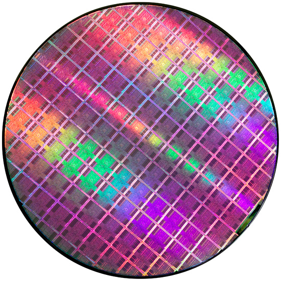
At most, 94 NVIDIA GT200 die can be produced on a single 300mm 65nm wafer from TSMC. On the other end of the spectrum, Intel can fit around 2500 45nm Atom processors on a 300mm wafer.
If the number of transistors wasn't enough to turn this thing into a dinner plate sized bit of hardware, the fact that it's fabbed on a 65nm process definitely puts it over the top. Current CPUs are at 45nm and NVIDIA's major competitor in the GPU market, AMD, has been building 55nm graphics chips for over 7 months now. With so many transistors, choosing not to shrink their manufacturing process doesn't seem to make much sense to us. Smaller fab processes offer not only the potential for faster, cooler chips, but also significantly reduce the cost of the GPU itself. Because manufacturing costs are (after ramping production) on a per wafer basis, the more dies that can be packed onto a single waffer, the less each die costs. It is likely that NVIDIA didn't want to risk any possible delays arising from manufacturing process changes on this cycle, but that seems like a risk that would have been worth taking in this case.
Instead, GT200 is the largest die TSMC has ever fabbed for production. Quite a dubious honor, and I wouldn't expect NVIDIA to really see this as something of which to be proud. Of course, that doesn't mean we can't be impressed with the sheer massiveness of the beast.
And what do we get from all these transistors? Moving up from 690M transistors of the original G80 and 754M transistors in G92 to the 1.4B transistors of GT200 is not a small tweak. One of the major new features is the ability to processes double precision floating point data in hardware (there are 30 64-bit FP units in GT200). The size of the register file for each SP array has been doubled. The promised ability of an SP to process a MAD and a MUL at the same time has been enhanced to work in more cases (G80 was supposedly able to do this, but the number of cases where it worked as advertised were extremely limited). And the number of SPs has increased from 128 on G80 to 240 with GT200. To better understand what all this means, we'll take a closer look at the differences between G80 and GT200, but first, the cards.
Clock Speeds, Pricing and HDMI Information
NVIDIA is introducing two GT200 parts today along with slightly tweaked branding. The new brand is called the GeForce GTX, and the first two cards are the GTX 280 and GTX 260.


Here's the card, say hello:
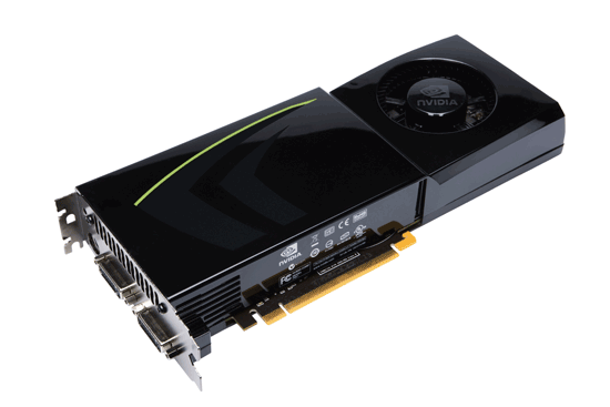
The GeForce GTX 280
It's got a little sibling too:

The GeForce GTX 260
The GeForce GTX 280 features 240 streaming processors running at 1.3GHz. It's got a 512-bit memory interface to 1GB of GDDR3 running at 2.2GHz (1107MHz core clock). The rest of the GPU runs at 602MHz.
| |
GTX 280 | GTX 260 | 9800 GX2 | 9800 GTX | 8800 GTS 512 | 8800 GT |
| Stream Processors | 240 | 192 | 256 | 128 | 128 | 112 |
| Texture Address / Filtering | 80 / 80 | 64 / 64 | 128 / 128 | 64 / 64 | 56 / 56 | 56 / 56 |
| ROPs | 32 | 28 | 32 | 16 | 16 | 16 |
| Core Clock | 602MHz | 576MHz | 600MHz | 675MHz | 650MHz | 600MHz |
| Shader Clock | 1296MHz | 1242MHz | 1500MHz | 1690MHz | 1625MHz | 1500MHz |
| Memory Clock | 1107MHz | 999MHz | 1000MHz | 1100MHz | 970MHz | 900MHz |
| Memory Bus Width | 512-bit | 448-bit | 256-bit x 2 | 256-bit | 256-bit | 256-bit |
| Frame Buffer | 1GB | 896MB | 1GB | 512MB | 512MB | 512MB |
| Transistor Count | 1.4B | 1.4B | 1.5B | 754M | 754M | 754M |
| Manufacturing Process | TSMC 65nm | TSMC 65nm | TSMC 65nm | TSMC 65nm | TSMC 65nm | TSMC 65nm |
| Price Point | $650 | $400 | $500 | $300 | $280 | $170-$230 |
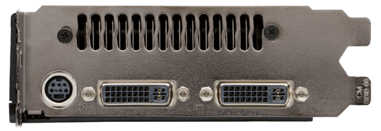
You'll need a power supply that can deliver up to 236W for the card itself and you'll need both a 6-pin and an 8-pin PCIe power connector (the board won't work with two 6-pin connectors).
The GeForce GTX 280 will retail for $650 with availability planned for June 17th.
The GTX 260 brings the total core count down to 192 by disabling two Texture/Processing Clusters on the GPU (but still maintaining more cores than any single-GPU G80/G92 based card). The SPs run slightly slower on the GTX 260 (1242MHz vs. 1296MHz, NVIDIA uses a 27MHz crystal so that's why we get these funny clock frequencies), while the memory runs at approximately 2GHz (999MHz memory clock, 1998MHz data rate). The GTX 260 also loses one of the 8 64-bit memory controllers, bringing the total memory bus down to 448-bits and total memory size down to 896MB.
The GTX 260 consumes a maximum of 183W and only needs two 6-pin power connectors. The GeForce GTX 260 will set you back $400 and should be available on June 26th.
The GTX 280's shroud, though it takes some cues from the 9800 GX2, is better engineered to allow for heat expulsion through a larger vent next to the IO ports. The 9800 GX2 didn't have a very wide opening to the outside world from which to remove heat. This resulted in the 9800 GX2 disproportionately increasing the heat of the system. Since we run our systems without cases we don't see problems like this as soon as our readers do, and we would like to thank you for pointing this out to us.
Both the GTX 260 and 280 have two dual-link DVI outputs, which can be converted to HDMI using an adapter if you'd like. You can pass SPDIF using a connector at the top of the card, which will then be passed to the HDMI output when using the DVI-HDMI adapter. For the HTPC enthusiasts out there, the GTX 280 and 260 can output the following audio formats over HDMI:
2-channel LPCM
6-channel DD bitstream
6-channel DTS bitstream
Unfortunately there's no support for 8-channel LPCM or bitstreaming of Dolby TrueHD or DTS HD-MA.


108 Comments
View All Comments
elchanan - Monday, June 30, 2008 - link
VERY eye-opening discussion on TMT. Thank you for it.I've been trying to understand how GPUs can be competitive for scientific applications which require lots of inter-process communication, and "local" memory, and this appears to be an elegant solution for both.
I can identify the weak points of it being hard to program for, as well as requiring many parallel threads to make it practical.
But are there other weak points?
Is there some memory-usage profile, or inter-process data bandwidth, where the trick doesn't work?
Perhaps some other algorithm characteristic which GPUs can't address well?
Think - Friday, June 20, 2008 - link
This card is a junk bond when taking into consideration cost/perfomance/power consumption.Reminds me of a 1976 Cadillac with a 7.7litre v8 with only 210 horsepower/3600 rpm.
It's a PIG.
Margalus - Tuesday, June 24, 2008 - link
this shows how many people don't run a dual monitor setup. I would snatch up one of these 260/280's over the gx2's anyday, gladly!!The performance may not be quite as good as an sli setup, but it will be much better than a single card which is what a lot of us are stuck with since you CANNOT run a dual monitor setup with sli!!!!!!!!!!!!!!!!!!!!!!!!!!!!!!!!!!!!!!!!!!!!!!!!!!!!!!!!
iamgud - Wednesday, June 18, 2008 - link
"I can has vertex data"LOL
These look fine, but need to be moved to 55nm. By the time I save up for one they will .
calyth - Tuesday, June 17, 2008 - link
Well what the heck are they doing with 1.4B transistors, which is becoming the largest die that TMSC has been producing so far?The larger the core, the more likely that an blemish would take out the core. As far as I know, didn't Phenom (4 cores on die) suffered low-yield problems?
gochichi - Tuesday, June 17, 2008 - link
You know, when you consider the price and you look at the benchmarks, you start looking for features and NVIDIA just doesn't have the features going on at all.COD4 -- Ran perfect at 1920x1200 with last gen stuff (the HD3870 and 8800GT(S))so now the benchmarks have to be for outrageous resolutions that a handful of monitors can handle (and those customers already bought SLI or XFIRE, or GTX2 etc.)
Crysis is a pig of a game, but it's not that great (it is a good technical preview though, I admit), and I don't think even these new cards really satisfy this system hog... so maybe this is a win, but I doubt too many people care... if you had an 8800GT or whatever, you're already played this game "well enough" on medium settings and are plenty tired of it. Though we'll surely fire it up in the future once our video cards "happen to be able to run it on high" very few people are going to go out of their way $500+ for this silly title.
In any case, then you look at ATI, and they have the HDMI audio, the DX 10.1 support and all they have to do at this point is A) Get a good price out the door, B) Make a good profit (make them cheap, which these NVIDIA are expensive to make, no doubt) and C) handily beat the 8800GTS and many of us are going to be sold.
These cards are what I would call a next gen preview. Some overheated prototypes of things to come. I doubt AMD will be as fast, and in fact I hope they aren't just as long as they keep the power consumption in check, the price, and the value (HDMI, DX10.1, etc).
Today's release reminded me that NVIDIA is the underdog, they are the company that released the FX series (desperate technology, like these are). ATI has been around well before 3DFX made 3d-accelerators. They were down for a bit, and we all said it was over for ATI but this desperate release from NVIDIA makes me think that ATI is going to be quite tought to beat.
Brazofuerte - Tuesday, June 17, 2008 - link
Can I go somewhere to find the exact settings used for these benchmarks? I appreciate the tech side of the write up but when it comes to determining whether I want one of these for my gaming machine (I ordered mine at midnight), I find HardOCP's numbers much more useful.woofermazing - Tuesday, June 17, 2008 - link
AMD/ATI isn't going to abandon the high end like your article implies. Their plan is to make a really good mid range chip, and ductape to cores together ala the X2's. Nvidia goes from the high-end down, ATI from the mid-end up. From the look of it, ATI might have the right idea, atleast this time around. I seriously doubt we'll see a two core version of this monster anytime soon.DerekWilson - Tuesday, June 17, 2008 - link
they are abandoning the high end single GPU ...we did state that they are planning on competing in the high end space with multiGPU cards, but that there are drawbacks to that.
we'll certainly have another article coming out sometime soon that looks a little more closely at AMD's strategy.
KeypoX - Tuesday, June 17, 2008 - link
i dont like it, not impressed either :(. Hopefully my 8800gt last for a while, far past this crap atleast