PCI Express 2.0: Scalable Interconnect Technology, TNG
by Kris Boughton on January 5, 2008 2:00 AM EST- Posted in
- CPUs
PCI Express Link Speeds and Bandwidth Capabilities
PCI Express uses a highly scalable architecture that is capable of delivering high bandwidth with a relatively low pin-count, dramatically simplifying design complexity while simultaneously allowing for smaller interface footprints. This is accomplished through the use of Low Voltage Differential Signal (LVDS) signal pairs - a simple two wire connection allowing for 1 bit to be transferred per clock (therefore 1GT/s is equal to 1Gbps). A pair per direction makes bi-directional signaling possible, which effectively doubles the throughput to 2 bits per cycle. Together these four pins comprise a single "lane." No additional pins are needed for data transfer as the clock signal is transmitted using these same pins through the use of an encoding scheme known as 8b/10b encoding. Without getting into too much detail this means that 8 bits of data are transferred using a 10-bit signal. While this does add 25% overhead to each data transfer, it eliminates the need to route separate traces for clock signals, the downside being that the maximum throughput is reduced by about 20%. Because the clock rate is so high (2.5GHz), the PCI Express protocol is able to transfer up to 500MB/s of bi-directional data with just four pins (compared to the legacy PCI bus which transfers 133MB/s of data using 32 pins). Higher data transfer rates require either the use of numerous parallel traces or increased clocking rates - in this case we can see that the tradeoff has been clearly been made in favor of a low-pin count.
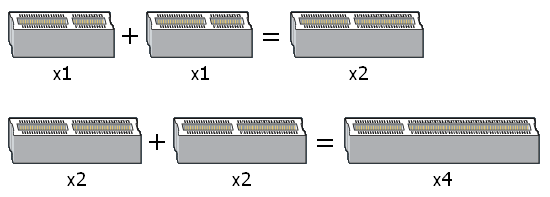
Multiple lanes can be grouped through a method knows as training, wherein the downstream device and the host negotiate how many lanes will be assigned. Although plugging a PCI Express card into a slot smaller than itself is not physically possible, plugging into a larger slot is mechanically possible. During training, the host device simply queries the device for its maximum link speed and assigns resources as needed. (Keep in mind that link speed is a bit of a misnomer - the PCI Express physical link layer always operates at the same frequency; it's the number of assigned lanes that changes). This method becomes a little more complicated in the case where the mechanical size of the slot does not necessarily match the host's maximum offered link speed. For example, many of today's X38-based motherboards include a third x16 slot but are only capable of providing x4 bandwidth (PCI Express 1.x) - more on why this is later. In this case, the installed device must be willing to operate at a reduced link speed. The PCI Express interface supports interconnect widths of x1, x2, x4, x8, x16, and x32. As an aside, PCI-E x32 slots are rarely seen because of their exceptional length, but thanks to PCI Express 2.0 we can now get the same bandwidth in PCI-E x16 form factor.
The part of the installed card's edge connector to the left of the key notch is always the same, no matter the card. Power, ground, reference voltages, and pads for control, training, and link maintenance are located here and are the required minimum required for operation. Data transfers to and from the device are accomplished using repeating blocks of pads - those that form the signals that comprise a single lane. The longer the slot is from the right of the keyway the higher the speed it offers (this assumes that it does in fact offer a maximum link speed congruent with its mechanical size). This all makes determining a device's default link speed quite easy - a quick look at the length of the edge connector and you have everything you need to know.
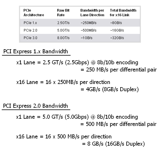
The table below compares PCI Express 1.x with 2.0 as well as 3.0 (which is now in the development stage - expect to see products based on this revision sometime in 2010). PCI Express 2.0 builds upon PCI Express 1.x primarily through the doubling of the clock rate to 5.0GHz (up from 2.5GHz). This brings to light an important point: earlier we noted that the PCI Express physical link layer always operates at the same speed. This is true except in the case where a PCI Express 1.x device is installed in a PCI Express 2.0 compliant slot - although the host is capable of the higher signaling frequency the device is not; the result being the use of the slower (2.5GT/s) clock rate. Note how the 8b/10b encoding overhead is factored into the actual usable bandwidth calculation.
Using PCI Express 2.0, motherboard designers can now either offer double the bandwidth in an equivalent size slot or can choose to create smaller layouts without sacrificing performance. In any case, this additional design flexibility paves the way for significant improvements in future products. PCI Express 3.0 will likely double the bandwidth provided by the previous generation again. You may have noticed though that the change must come from something more than just a decrease in the cycle time. This will be due a change in the encoding scheme - PCI-E 3.0 will stop using 8b/10b encoding, and whether or not the new scheme is truly more efficient than that used today remains to be seen. Expect the same level of backward-compatibility though as PCI-SIG is already assuring us that our then ancient PCI Express 1.x cards will run without difficulty in a PCI Express 3.0 slot. Let's take a closer look at exactly why they can make such a bold claim.


21 Comments
View All Comments
PhotoPrint - Sunday, May 11, 2008 - link
????? ?? ????????? ??????
????
?????
????? ??????
nubie - Monday, January 14, 2008 - link
I would like to point out that since the link auto-negotiates you can plug x16 cards into x8, x4, x2, and x1. The problem of physical connection is easily solved. I have done this two ways, one by cutting the back out of the motherboard connector, (seen here: http://picasaweb.google.com/nubie07/PCIEX1">http://picasaweb.google.com/nubie07/PCIEX1 ), and also by cutting the connector off of the video card down to x1 (sorry, no pics of this online). I did this to get 3 cards and 6 monitors on a standard (non SLI) motherboard. You can also purchase stand-offs from x16 to x8-x1, or modify a x1-x1 standoff (or "wearout" adaptor) to allow the x16 card to plug in.The throughput was more than enough, depending on your video cards on-board ram it can even play newer games fine. The utter lack of multi-head display support in DirectX and most games is just mind-boggling. Tell me why PC games won't allow multi-player, while consoles do?
cheburashka - Monday, January 7, 2008 - link
"and there is no obvious reason as to why 2x8 CrossFire on a P965 chipset should not work"It has a single LTSSM thus it can not be split into multiple ports.
cheburashka - Monday, January 7, 2008 - link
"and there is no obvious reason as to why 2x8 CrossFire on a P965 chipset should not work"It only has a single LTSSM thus it can not be split into multiple ports.
fredsky - Monday, January 7, 2008 - link
sorry guys to be not as enthusiast...http://www.fudzilla.com/index.php?option=com_conte...">http://www.fudzilla.com/index.php?optio...mp;task=...
there ARE a lot a issues here, especially with RAID cards pluged into PCIe 2 slots. LSI, 3Ware, Areca and so on.
anand can you make some tests ?
I read that Gigabyte GA-X38-DQ6 is compatible with Areca at least.
regards
fredsky
decalpha - Monday, January 7, 2008 - link
I am not sure who is the guilty party but my new and shiny 8800GT refuses to POST. And if you search the user forums it's clear that most of the problems are faced by socket 939 systems with nvidia chipset. In the end it's the user who suffers.Comdrpopnfresh - Monday, January 7, 2008 - link
Does PCI-E also increase the available current supplied to the card by the slot? Doubling seems to be a theme here... Maybe from 75-150 Watts? I skimmed, so I apologize if it was written or already mentioned...kjboughton - Monday, January 7, 2008 - link
Although we didn't discuss this in the article, I can certainly answer the question: no. The slot still supplies up to a maximum of 75W per the specification; however, the PCI Express Card Electromechanical interface spec will allow for an additional 150W power delivery via external power cables for a total of 225W. Anything above this number is technically out of specification.AndyHui - Sunday, January 6, 2008 - link
Didn't seem all that long ago when I wrote the first PCI Express article here on AT.... but looking back, that was 2003.Good article.... but I thought the official abbreviation was PCIe, not PCI-E?
saratoga - Saturday, January 5, 2008 - link
"PCI Express 3.0 should further increase the PCI-E Multiplier to 80x, which will bring the base link frequency very near the maximum theoretical switching rate for copper (~10Gbps)."This will be quite a surprise to the Ethernet people who can do 100 Gbit/s over 2 ethernet twisted pairs on their prototype systems! 500% of the theoretical maximum for copper is pretty good.
Theres no theoretical maximum for copper since in theory the SNR can be infinite, and thus you can keep coming up with better codes. Theres a practical limit, set by just how high you can get the SNR in a real circuit, but thats also unbelievably high. The real limit for a PC is how much power you're willing to commit to your increasingly complicated transmission system.