Samsung Starts 3nm Production: The Gate-All-Around (GAAFET) Era Begins
by Ryan Smith on June 30, 2022 6:00 AM EST- Posted in
- CPUs
- Samsung
- Semiconductors
- Samsung Foundry
- 3nm
- GAAFET
- MBCFET
- 3GAE
- 3GAP
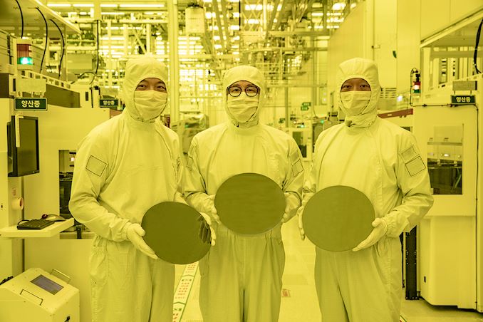
Capping off a multi-year development process, Samsung’s foundry group sends word this morning that the company has officially kicked off production on its initial 3nm chip production line. Samsung’s 3nm process is the industry’s first commercial production process node using gate-all-around transistor (GAAFET) technology, marking a major milestone for the field of silicon lithography, and potentially giving Samsung a major boost in its efforts to compete with TSMC.
The relatively spartan announcement from Samsung, which comes on the final day of Q2, announces that Samsung has begun production of chips on a GAAFET-enabled 3nm production line. The company is not disclosing the specific version of the node used here, but based on previous Samsung roadmaps, this is undoubtedly Samsung’s initial 3GAE process – essentially, Samsung’s earliest process node within a family. According to Samsung, the line will initially be used to produce chips for “high performance, low power computing”, with mobile processors to come later. Samsung’s early process nodes are traditionally reserved for the company’s internal use, so while Samsung isn’t announcing any specific 3nm chips today, it’s only a matter of time until we see a 3nm SoC announces from Samsung LSI.
Samsung has, for the most part, been quiet about its progress on 3nm/GAAFET this year. The last significant news we heard from the company on the matter was several months ago at the company’s Foundry Forum event, where the company reiterated plans to get 3GAE into production by the end of 2022. Given the previous silence and the cutting-edge nature of the technology, there had been more than some concern that 3GAE would be delayed past 2022 – adding on to delays that pushed the tech out of its original 2021 launch window – but with today’s announcement Samsung seems to want to put that to rest.
![]()
With that said, the devil is in the detail in these announcements, especially as to what’s said versus not said. Taken literally, today’s announcement from Samsung notably does not include any mention of “high volume” manufacturing, which is the traditional milestone for when a process node is ready for commercial use. So by merely saying 3nm is in production, Samsung’s announcement leaves the company with a fair bit of wiggle room with regards to just how many chips they’re capable of producing – and at what yields. The company was producing test chips back in 2021, so the matter is more nuanced than just firing up the fab, so the line between PR and productization is fuzzy, to say the least.
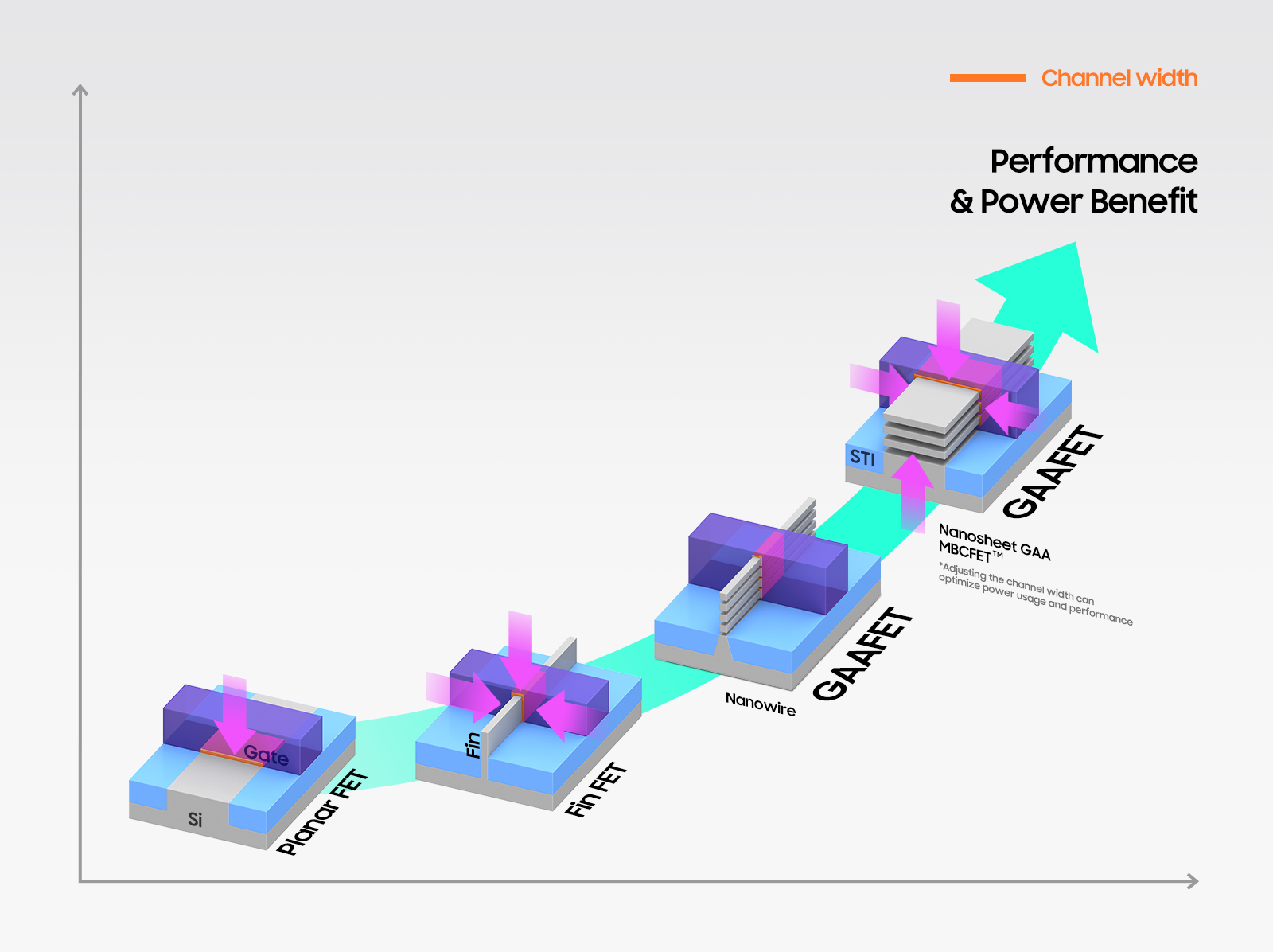
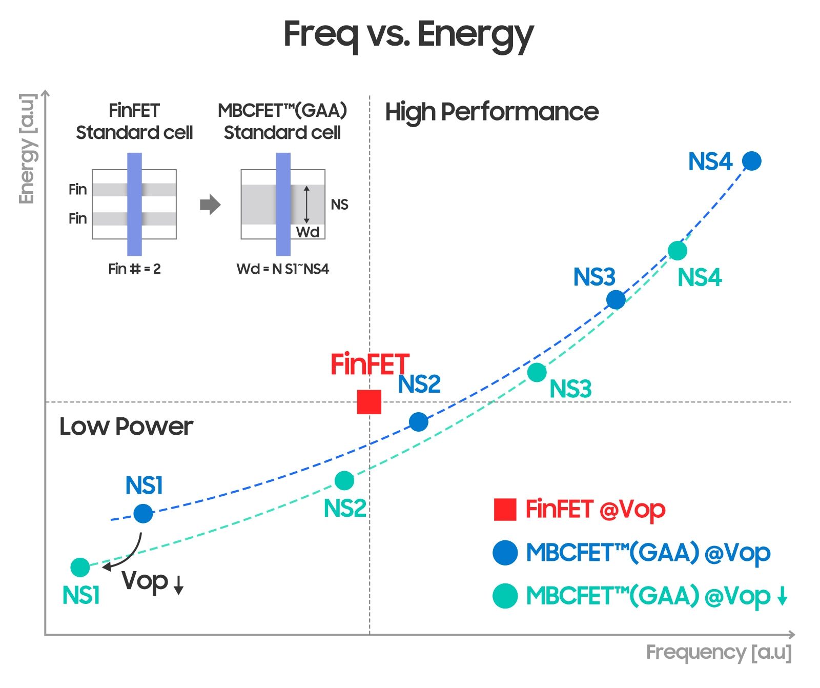
Still, today’s announcement is a major moment for Samsung, who has been working on 3nm/GAAFET technology since before 2019, when they initially announced the technology. Samsung’s specific flavor of GAA transistor technology is Multi Bridge Channel FET (MBCFET), which is a nanosheet-based implementation. Nanosheet-based FETs are extremely customizable, and the width of the nanosheet is a key metric in defining the power and performance characteristics: the higher the width, the higher the performance (at higher power). As a result, transistor designs that focus on low power can use smaller nanosheets, while logic that requires higher performance can go for the wider sheets.
Along with today’s production announcement, Samsung has also offered some updated size and performance figures comparing 3GAE to older nodes. Officially, 3GAE can offer 45% reduced power consumption or 23% improved performance compared to Samsung’s 5nm process (the company doesn’t state which flavor), with an overall reduction in feature size of 16%. These figures are notably different from Samsung’s previous (2019) figures, which compared the tech to Samsung’s 7LPP node. Given the change in baselines, it’s not clear at this point whether 3GAE is living up to Samsung’s initial claims, or if they’ve had to back off a bit for the initial version of their 3nm technology.
What is clear, however, is that Samsung has more significant improvements in mind for the second iteration of 3nm, which we know is 3GAP(lus). According to today’s press release, Samsung is expecting a 50% power reduction or 30% performance improvement versus the same 5nm baseline, with a much greater 35% area reduction. Today’s announcement doesn’t offer a date for 3GAP, but per previous roadmaps, 3GAP is expected to land around a year after 3GAE. 3GAP is also when we expect to see Samsung open the door to outside customers, though given the harsh competitive environment, nothing should be taken for granted.

Samsung Process Roadmap (July 2021)
The launch of Samsung’s 3nm process tech comes as the company is working to regain its footing against arch rival TSMC, who has clearly pulled into the lead in the 5nm/4nm generation. The gap between TSMC and Samsung has been wide enough that major customers such as Qualcomm have been porting high-performance chips like the Snapdragon 8 series from Samsung to TSMC, and at this point Samsung has seen few major 5nm/4nm wins compared to TSMC. If everything goes well, being the first fab with GAAFET tech could give Samsung a temporary-but-material advantage over TSMC, whose 3nm process is still using older FinFET-style transistors. But in order to pull that off, Samsung will need to reverse their earlier technical problems and deliver a performant, high-yielding process that’s far enough ahead to woo skeptical customers.


Source: Samsung


21 Comments
View All Comments
Wereweeb - Thursday, June 30, 2022 - link
Hoping Samsung can get their shit together so someone can compete with TSMC.nandnandnand - Thursday, June 30, 2022 - link
Even if their nodes have been worse than TSMC's, they are only moderately behind. As long as they don't drop out of the race entirely like GlobalFoundries did, things are fine.FreckledTrout - Thursday, June 30, 2022 - link
Exactly this. If you are a little behind, you compete on price which is no big deal. Somone has to be behind at any point. Ideally Samsung, TSMC and Samsung would start leapfrogging each other.dersteffeneilers - Sunday, July 31, 2022 - link
did you read the interview with Tom Caufield, explaining why they were pulling out? Paraphrasing here, he said that if you're not first in the foundry business, you might as well be last. If you have the money to design cutting edge chips, you can spend the extra money to go leading edge. AMD must have gotten a heads up before GF pulled out. If they were interested, why didn't they just bankroll 7nm development?sharath.naik - Thursday, June 30, 2022 - link
This is especially needed given Taiwan will be annexed by china any time now.shabby - Thursday, June 30, 2022 - link
Uncle Joe won't let that happen 😂Wereweeb - Friday, July 1, 2022 - link
China started conquering Taiwan around 1683. If you mean the PRC government annexing the ROC government, I very much doubt it. Russia is getting sanctioned back to the stone age for trying to blitz into Donbas and Ukraine.Vitor - Friday, July 1, 2022 - link
Russia is a much smaller market than China. Most companies can boycott it just fine. China is much, much larger. Way too much money involved for companies to give up because of commies doing atrocitiesKhanan - Monday, July 4, 2022 - link
Source or just talking nonsense?andychow - Friday, July 29, 2022 - link
Have you been living under a rock?