TSMC Update: 2nm in Development, 3nm and 4nm on Track for 2022
by Anton Shilov on April 26, 2021 2:15 PM EST
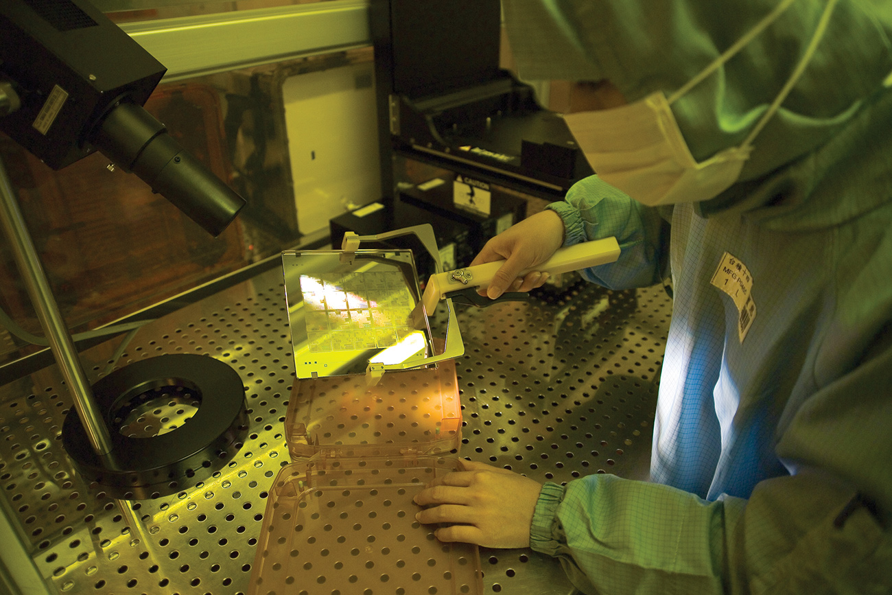
For TSMC, being the world's largest foundry with nearly 500 customers has its peculiarities. On the one hand, the company can serve almost any client with almost any requirements. On the other hand, it has to stay ahead of everyone else both in terms of capacity and in terms of technology. As far as capacity is concerned, TSMC is unchallenged and is not going to be for years to come. As for fabrication technologies, TSMC has recently reiterated that it's confident that its N2, N3, and N4 processes will be available on time and will be more advanced than competing nodes.
Confidence
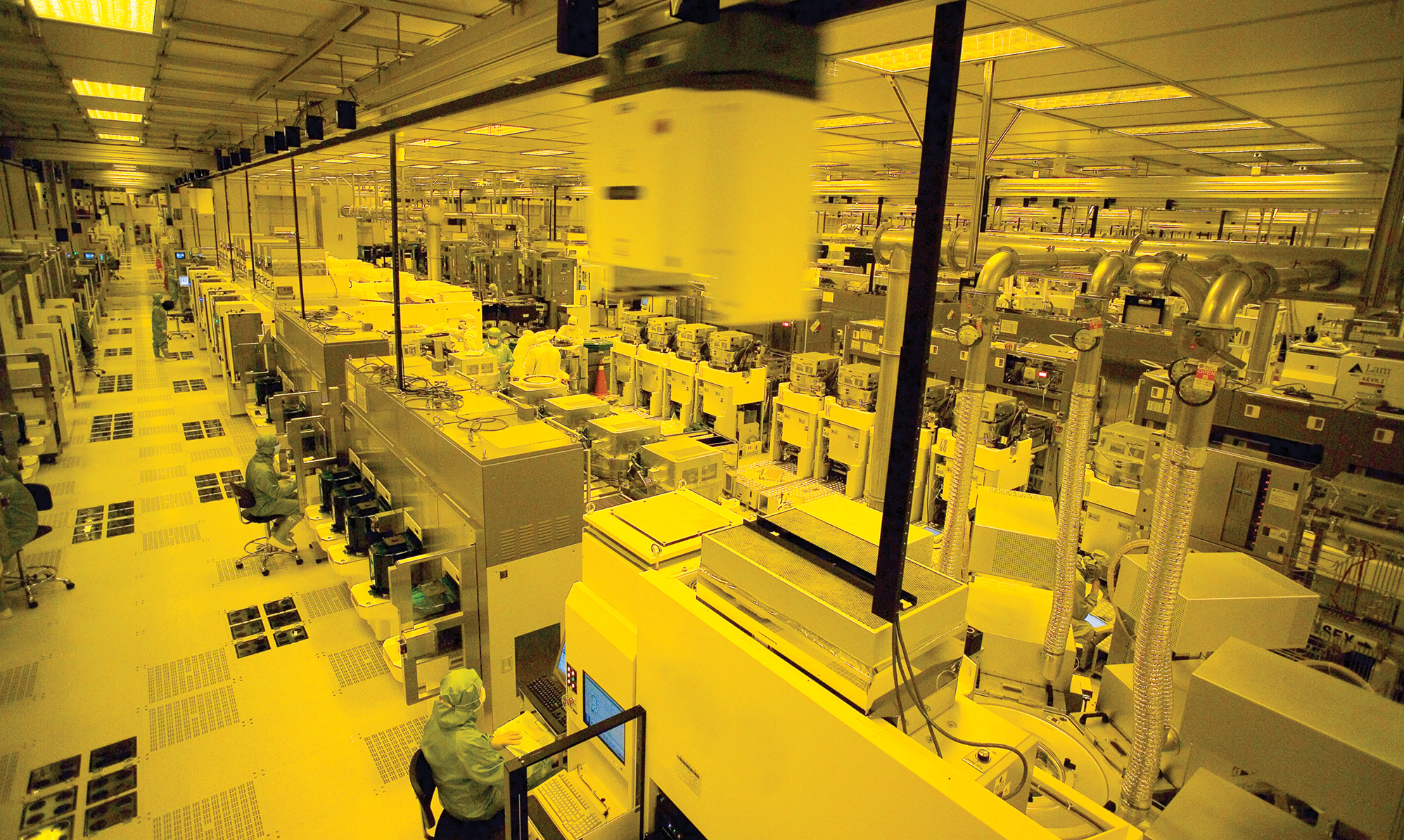
Early this year TSMC significantly boosted its 2021 CapEx budget to a $25 – $28 billion range, further increasing it to around $30 billion as a part of its three-year plan to spend $100 billion on manufacturing capacities and R&D.
About 80% of TSMC's $30 billion capital budget this year will be spent on expanding capacities for advanced technologies, such as 3nm, 4nm/5nm, and 6nm/7nm. Analysts from China Renaissance Securities believe that most of the money on advanced nodes will be used to expand TSMC's N5 capacity to 110,000 ~ 120,000 wafer starts per month (WSPM) by the end of the year. Meanwhile, TSMC said that 10% of its CapEx will be allocated for advanced packaging and mask making, whereas another 10% will be spent on specialty technologies (which includes tailored versions of mature nodes).
TMSC's the most recent CapEx hikes announcements were made after Intel announced its IDM 2.0 strategy (that involves in-house production, outsourcing, and foundry operations) and to a large degree reaffirms TMSC's confidence in both short-term and long-term future even ahead of intensified competition.
"As a leading pure-play foundry, TSMC has never been short on competition in our 30-plus-year history, yet we know how to compete," said C.C. Wei, president and CEO of TSMC, at a recent conference call with analysts and investors. "We will continue to focus on delivering technology leadership, manufacturing excellence, and earning our customers' trust. The last point, customers' trust, is fairly important because we do not have internal products that compete with customer."
| Advertised PPA Improvements of New Process Technologies Data announced during conference calls, events, press briefings and press releases |
|||||||||
| TSMC | |||||||||
| N7 vs 16FF+ |
N7 vs N10 |
N7P vs N7 |
N7+ vs N7 |
N5 vs N7 |
N5P vs N5 |
N4 vs N5 |
N3 vs N5 |
||
| Power | -60% | <-40% | -10% | -15% | -30% | -10% | lower | -25-30% | |
| Performance | +30% | ? | +7% | +10% | +15% | +5% | higher | +10-15% | |
| Logic Area Reduction % (Density) |
70% |
>37% |
- |
~17% |
0.55x -45% (1.8x) |
- |
? | 0.58x -42% (1.7x) |
|
| Volume Manufacturing |
2018 | 2018 |
2019 | Q2 2019 |
Q2 2020 | 2021 | 2022 | H2 2022 | |
N5 Gaining Customers
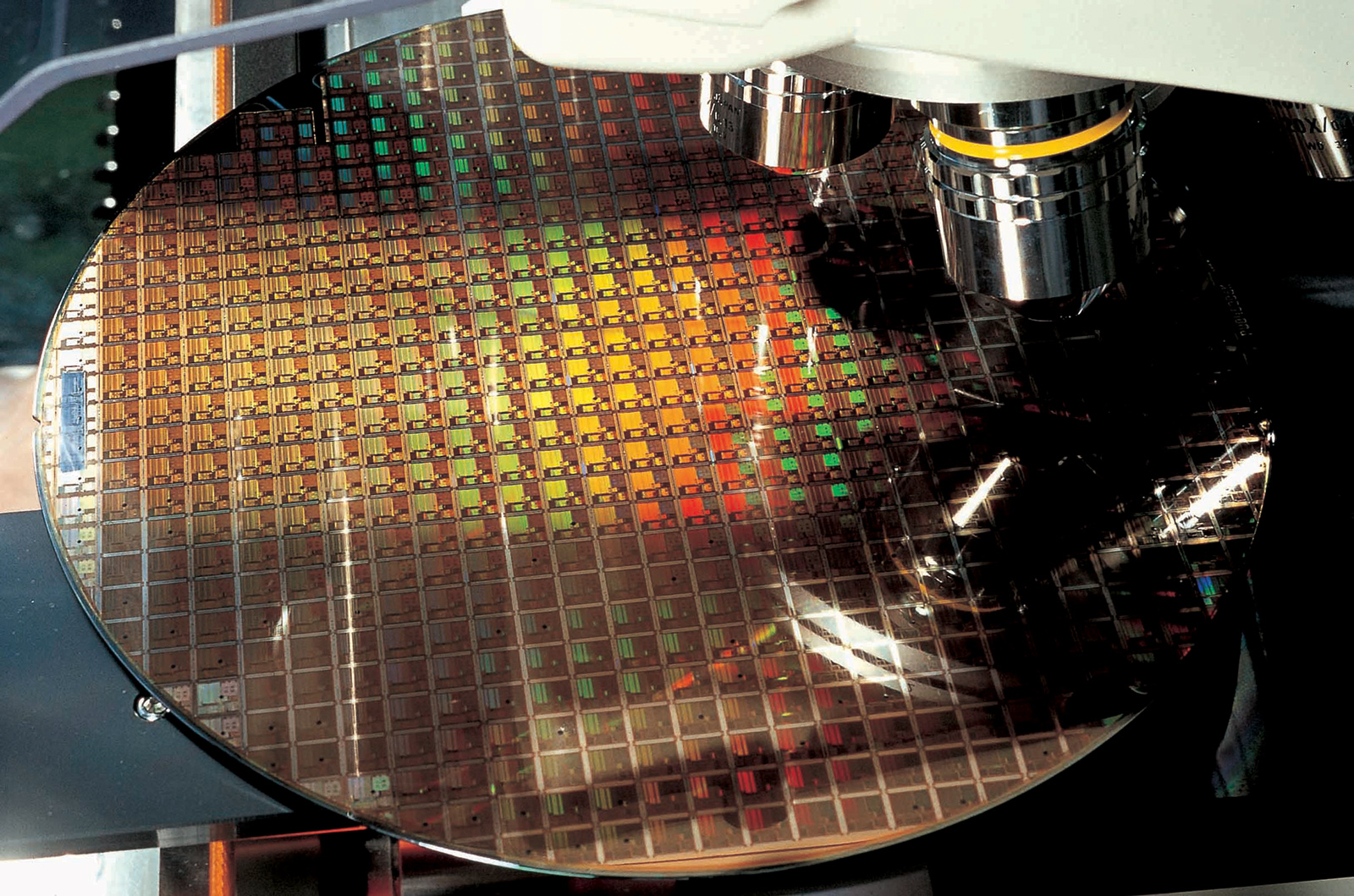
TSMC was the first company to start high volume manufacturing (HVM) of chips using its N5 (5 nm) process technology in mid-2020.
Initially, the node was used solely for TSMC's alpha customers — Apple and HiSilicon. Shipments to the latter ceased on September 14, which left all of the leading-edge capacity to Apple. By now, more customers are ready with their N5 designs, so the adoption of this node is growing. Meanwhile, TSMC says more customers are planning to use N5 family of technologies (including N5, N5P, and N4) than it expected just several months ago.
"N5 is already in its second year of volume production with yield better than our original plan," said Mr. Wei. N5 demand continues to be strong, driven by smartphone and HPC applications, and we expect N5 to contribute around 20% of our wafer revenue in 2021. […] In fact, we are seeing stronger engagement with more customers on 5 nm and 3 nm [versus 7 nm at similar stages]. The engagement is so strong that we have to really prepare the capacity for it."
For TSMC, HPC applications include many different types of products, including AI accelerators, CPUs, GPUs, FPGAs, NPUs, and video gaming SoCs, just to name a few. Since they're just a contract manufacturer, TSMC does not disclose what kinds of products it makes using one node or another (we do know that it builds the Apple A14 SoC for smartphones/tablets/STBs as well as the Apple M1 SoC for PCs and tablets), but the very fact that adoption of N5 is growing in the HPC segment is important.
"We expect demand for our N5 family to continue to grow in the next several years, driven by the robust demand for smartphone and HPC applications," the head of TSMC said. "We expect to see HPC, not only in the first wave, but in additional waves of demand to support our leading [N5] node in the future, actually."
It is not particularly surprising that TSMC's N5 is gaining market share among adopters of leading-edge technologies. Analysts from China Renaissance estimate that TSMC's N5 features a transistor density of around 170 million transistors per square millimeter (MTr/mm2), which if accurate, makes it the densest technology available today. By contrast, Samsung's Foundry's 5LPE can boast with about 125 MTr/mm2 ~130 MTr/mm2, whereas Intel's 10 nm features an approximately 100 MTr/mm2 density.
In the coming weeks TSMC is set to start making chips using a performance-enhanced version of its N5 technology called N5P that promises to increase frequencies by up to 5% or reduce power consumption by up to 10% (at the same complexity). The technology offers a seamless migration path for customers without requiring significant engineering resource investment or longer design cycle time, so anyone with an N5 design can use N5P instead. For example, early adopters of N5 could re-use their IP for their N5P chips.
N4: On Track for Next Year
TSMC's N5 family of technologies also includes evolutionary N4 process that will enter risk production later this year and will be used for mass production in 2022.
This technology is set to provide further PPA (power, performance, area) advantages over N5, but keep the same design rules, design infrastructure, SPICE simulation programs, and IPs. Meanwhile, since N4 further extends usage of EUV lithography tools, it also reduces mask counts, process steps, risks, and costs.
"N4 will leverage the strong foundation of N5 to further extend our 5 nm family," said Mr. Wei. "N4 is a straightforward migration from N5 with compatible design rules while providing further performance, power and density enhancement for the next wave of 5-nanometer products. N4 risk production is targeted for second half this year and volume production in 2022."
By the time N4 enters HVM in 2022, TSMC will have about two years of experience with N5 and three years of experience with EUV. So expectations are that yields will be high and the performance variability promises to be low.
But even as cutting-edge as N4 is slated to be, it's not going to be the most advanced fabrication technology that TSMC will offer next year.
N3: Due in H2 2022
In 2022, the world's largest contract maker of chips will roll out its brand-new N3 manufacturing process, which will keep using FinFET transistors, but is expected to offer the whole package of PPA improvements.
In particular, versus their current N5 process, TSMC's N3 promises to increase performance by 10% – 15% (at the same power and complexity) or reduce power consumption by 25% – 30% (at the same performance and complexity). All the while the new node will also improve transistor density by 1.1 ~ 1.7 times depending on the structures (1.1X for analog, 1.2X for SRAM, 1.7X for logic).
N3 will further increase the number of EUV layers, but will keep using DUV lithography. Also, since the technology keeps using FinFET, it will not require a new generation of electronic design automation (EDA) tools redesigned from scratch and development of all-new IPs, which might become a competitive advantage over Samsung Foundry's GAAFET/MBCFET-based 3GAE.
"N3 will be another full node stride from our N5 and will use FinFET transistor structure to deliver the best technology maturity, performance, and cost for our customers," said Mr. Wei. "Our N3 technology development is on track with good progress. We continue to see a much higher level of customer engagement for both HPC and smartphone applications at N3 as compared with N5 and N7."
In fact, TSMC's claims about growing customer engagement with N3 indirectly telegraphs its high expectations for N3.
"[N3] risk production is scheduled in 2021," said TSMC's CEO. "The volume production is targeted in second half of 2022. Our N3 technology will be the most advanced foundry technology in both PPA and transistor technology, when it is introduced. […] We are confident that both our [N5] and [N3] will be large and long-lasting nodes for TSMC."
Beyond N3
Gate-all-around FETs (GAAFETs) are still a part of TSMC's development roadmap. The company is expected to use a new kind of transistors with its 'post-N3' technology (presumably N2). In fact, the company is in path-finding mode for next generations of materials and transistor structures that will be used many years down the road.
"For advanced CMOS logic, TSMC’s 3nm and 2nm CMOS nodes are progressing nicely through the pipeline," the company said in its annual report recently. "In addition, TSMC's reinforced exploratory R&D work is focused on beyond-2nm node and on areas such as 3D transistors, new memory and low-R interconnect, which are on track to establish a solid foundation to feed into many technology platforms.
It is noteworthy that TSMC is expanding capacity for R&D operations at Fab 12, where N3, N2, and more advanced nodes are currently being researched and developed.
Summary
Overall, TSMC is confident that its "everyone's foundry" strategy will enable it grow further in terms of scale, market share, and sales. The company also expects to maintain its technology leadership going forward, which is pivotal for growth.
"For the full year of 2021, we now forecast […] foundry industry growth [at] about 16%," said Wendell Huang, CFO of TSMC, at a recent conference call with analysts and investors. "For TSMC, we are confident we can outperform the foundry revenue growth and grow by around 20% in 2021."
The company has a strong technology roadmap and it is set to continue introducing improved leading-edge nodes every year, thus offering its customers improvements at a predictable cadence.
TSMC knows how to compete against rivals with leading-edge nodes as well as makers of chips focused on specialty process technologies, so it does not see Intel Foundry Services (IFS) as an immediate threat especially because the blue giant is going primarily after leading-edge and advanced nodes.
Financial analysts generally share TSMC's optimism mainly because of the expectation that the company's N3 and N5 nodes are not going to have competitors offering similar transistor densities and wafer starts.
"Following Intel's announced foundry comeback in March, TSMC’s willingness to set a 3-year $100 billion CapEx/R&D investment plan, starting from 2021, indicates its confidence to widen its foundry leadership," Szeho Ng, an analyst with China Renaissance Securities. "We see TSMC’s strategic value rising with N3/N5: strong N5 tape-out activities from HPC/smartphone applications and more N3 client engagement vs N5/N7 at similar stages."


74 Comments
View All Comments
Duncan Macdonald - Monday, April 26, 2021 - link
TSMC telling Intel that there is no way that Intel can catch them.(I wonder how the performance of AMD CPUs on N3 will compare to Intel's CPUs on 14/10/7 nm.)
EthiaW - Monday, April 26, 2021 - link
Intel would better pray for China to launch the attack ASAP. Nothing else can save it from the AMD+TSMC juggernaut.danjw - Monday, April 26, 2021 - link
It seems to me, that the greatest threat to both Intel and AMD is ARM. Not either to each other.dullard - Monday, April 26, 2021 - link
Exactly. People here don't realize that AMD and Intel are on the same team. The true struggle is AMD + Intel vs ARM.bcronce - Tuesday, April 27, 2021 - link
I used to consider ARM not competitive with Intel and AMD, but ARM is running around unchecked, rapidly moving towards desktops while maintaining their iron grip on mobile and embedded.icedeocampo - Wednesday, May 5, 2021 - link
But if AMDs does what it did with the x64 x86 discussion- we're all in for a treat - AMD can probably do a hybrid ARM x64 chip.MiauwMing - Wednesday, May 5, 2021 - link
Right. As if AMD or Intel doesn't produce or use any ARM CPUs. Every Ryzen CPU's utilize ARM cpu (for security). Intel uses ARM SOC for their FPGA products.https://www.intel.in/content/www/in/en/products/sk...
Matthias B V - Tuesday, April 27, 2021 - link
Agreed. They lose market share in servers and mobile applications like Notebooks fast. Desktop is in x86 hands so far but only a minor market.Wonder if AMD and Intel would work together to create a "Lean86" version of x86 that gets rid of legacy or only emulates it. It would free up die space a lot. Also I would love to see SVE on x86.
Lean x86 + SVE # bigLITTLE could help x86 to extend its life or survive but for now I see it dead by 2030.
What might safe them too is Nvidia really being able to buy ARM and other customers rather trandition to RISC-v. At least it helps until RISC-V kills both: ARM and x86!
TheinsanegamerN - Tuesday, April 27, 2021 - link
ARM has almost 0 presence in both desktops and notebooks. WTF are you talking about? ARM has never been able to sucessfully break into high power markets, they've had roughly the same luck as intel getting into ultra low power markets."lean 86" is already here. The x86 code, as has been discussed many times on many pages, is a tiny portion of modern core design and is already digested in small chunks like all other instructions. It isnt some big monolith that dominates cores like the 486 days.
It's funny, I remember reading in 2010 how by 2020 ARM would be a major industry player. Qualcomm was making some noise about entering the server market, AMD bought Seamicro, developed the K12 platform, then did nothing with it. Now the lines in "x86 will be dead by 2030"? I cant wait to see how utterly wrong that prediction is as well.
bcronce - Tuesday, April 27, 2021 - link
I guess you haven't heard of Apple's M1 CPU that is going to be in nearly all of their devices? It uses ARM for the compute cores.