Intel 3rd Gen Xeon Scalable (Ice Lake SP) Review: Generationally Big, Competitively Small
by Andrei Frumusanu on April 6, 2021 11:00 AM EST- Posted in
- Servers
- CPUs
- Intel
- Xeon
- Enterprise
- Xeon Scalable
- Ice Lake-SP
SPECjbb MultiJVM - Java Performance
Moving on from SPECCPU, we shift over to SPECjbb2015. SPECjbb is a from ground-up developed benchmark that aims to cover both Java performance and server-like workloads, from the SPEC website:
“The SPECjbb2015 benchmark is based on the usage model of a worldwide supermarket company with an IT infrastructure that handles a mix of point-of-sale requests, online purchases, and data-mining operations. It exercises Java 7 and higher features, using the latest data formats (XML), communication using compression, and secure messaging.
Performance metrics are provided for both pure throughput and critical throughput under service-level agreements (SLAs), with response times ranging from 10 to 100 milliseconds.”
The important thing to note here is that the workload is of a transactional nature that mostly works on the data-plane, between different Java virtual machines, and thus threads.
We’re using the MultiJVM test method where as all the benchmark components, meaning controller, server and client virtual machines are running on the same physical machine.
The JVM runtime we’re using is OpenJDK 15 on both x86 and Arm platforms, although not exactly the same sub-version, but closest we could get:
EPYC & Xeon systems:
openjdk 15 2020-09-15

OpenJDK Runtime Environment (build 15+36-Ubuntu-1)

OpenJDK 64-Bit Server VM (build 15+36-Ubuntu-1, mixed mode, sharing)
Altra system:
openjdk 15.0.1 2020-10-20

OpenJDK Runtime Environment 20.9 (build 15.0.1+9)

OpenJDK 64-Bit Server VM 20.9 (build 15.0.1+9, mixed mode, sharing)
Furthermore, we’re configuring SPECjbb’s runtime settings with the following configurables:
SPEC_OPTS_C="-Dspecjbb.group.count=$GROUP_COUNT -Dspecjbb.txi.pergroup.count=$TI_JVM_COUNT -Dspecjbb.forkjoin.workers=N -Dspecjbb.forkjoin.workers.Tier1=N -Dspecjbb.forkjoin.workers.Tier2=1 -Dspecjbb.forkjoin.workers.Tier3=16"
Where N=160 for 2S Altra test runs, N=80 for 1S Altra test runs, N=112 for 2S Xeon 8280, N=56 for 1S Xeon 8280, and N=128 for 2S and 1S on the EPYC system. The 75F3 system had the worker count reduced to 64 and 32 for 2S/1S runs.
The Xeon 8380 was running at N=140 for 2S Xeon 8380 and N=70 for 1S - the benchmark had been erroring out at higher thread counts.
In terms of JVM options, we’re limiting ourselves to bare-bone options to keep things simple and straightforward:
EPYC & Altra systems:
JAVA_OPTS_C="-server -Xms2g -Xmx2g -Xmn1536m -XX:+UseParallelGC "

JAVA_OPTS_TI="-server -Xms2g -Xmx2g -Xmn1536m -XX:+UseParallelGC"

JAVA_OPTS_BE="-server -Xms48g -Xmx48g -Xmn42g -XX:+UseParallelGC -XX:+AlwaysPreTouch"
Xeon Cascade Lake systems:
JAVA_OPTS_C="-server -Xms2g -Xmx2g -Xmn1536m -XX:+UseParallelGC"

JAVA_OPTS_TI="-server -Xms2g -Xmx2g -Xmn1536m -XX:+UseParallelGC"

JAVA_OPTS_BE="-server -Xms172g -Xmx172g -Xmn156g -XX:+UseParallelGC -XX:+AlwaysPreTouch"
Xeon Ice Lake systems (SNC1):
JAVA_OPTS_C="-server -Xms2g -Xmx2g -Xmn1536m -XX:+UseParallelGC"

JAVA_OPTS_TI="-server -Xms2g -Xmx2g -Xmn1536m -XX:+UseParallelGC"

JAVA_OPTS_BE="-server -Xms192g -Xmx192g -Xmn168g -XX:+UseParallelGC -XX:+AlwaysPreTouch"
Xeon Ice Lake systems (SNC2):
JAVA_OPTS_C="-server -Xms2g -Xmx2g -Xmn1536m -XX:+UseParallelGC"

JAVA_OPTS_TI="-server -Xms2g -Xmx2g -Xmn1536m -XX:+UseParallelGC"

JAVA_OPTS_BE="-server -Xms96g -Xmx96g -Xmn84g -XX:+UseParallelGC -XX:+AlwaysPreTouch"
The reason the Xeon CLX system is running a larger back-end heap is because we’re running a single NUMA node per socket, while for the Altra and EPYC we’re running four NUMA nodes per socket for maximised throughput, meaning for the 2S figures we have 8 backends running for the Altra and EPYC and 2 for the Xeon, and naturally half of those numbers for the 1S benchmarks.
For the Ice Lake system, I ran both SNC1 (one NUMA node) as SNC2 (two nodes), with the corresponding scaling in the back-end memory allocation.
The back-ends and transaction injectors are affinitised to their local NUMA node with numactl –cpunodebind and –membind, while the controller is called with –interleave=all.
The max-jOPS and critical-jOPS result figures are defined as follows:
"The max-jOPS is the last successful injection rate before the first failing injection rate where the reattempt also fails. For example, if during the RT-curve phase the injection rate of 80000 passes, but the next injection rate of 90000 fails on two successive attempts, then the max-jOPS would be 80000."
"The overall critical-jOPS is computed by taking the geomean of the individual critical-jOPS computed at these five SLA points, namely:
• Critical-jOPSoverall = Geo-mean of (critical-jOPS@ 10ms, 25ms, 50ms, 75ms and 100ms response time SLAs)
During the RT curve building phase the Transaction Injector measures the 99th percentile response times at each step level for all the requests (see section 9) that are considered in the metrics computations. It then computes the Critical-jOPS for each of the above five SLA points using the following formula:
(first * nOver + last * nUnder) / (nOver + nUnder) "
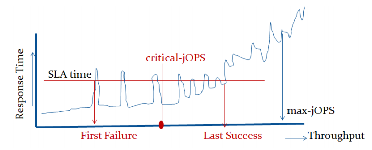
That’s a lot of technicalities to explain an admittedly complex benchmark, but the gist of it is that max-jOPS represents the maximum transaction throughput of a system until further requests fail, and critical-jOPS is an aggregate geomean transaction throughput within several levels of guaranteed response times, essentially different levels of quality of service.
Beyond the result figures, the benchmark keeps detailed track of timings of responses and tracks a few important statistical data-points across a response-time curve, as follows:
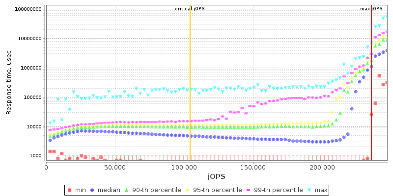
2S Xeon 8380 THP Enabled

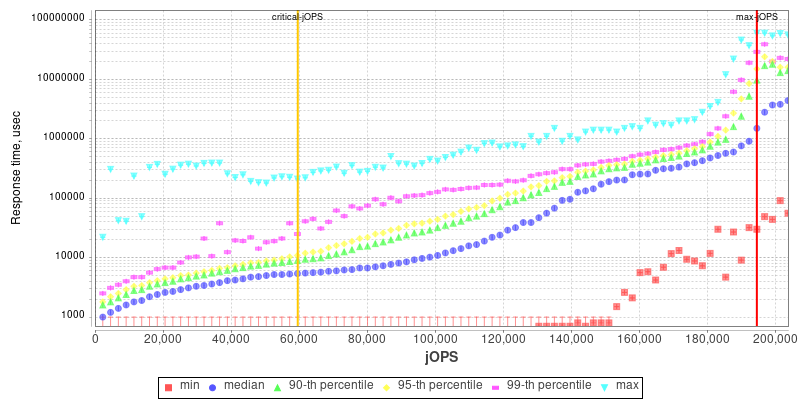
2S Xeon 8280 THP Enabled
Comparing the Xeon 8380 to the Xeon 8280, what’s to be immediately noted is the much-improved maximum throughput figure of the new part, scaling at +64% compared to its predecessor. We’re seeing that the load slope where the 99th percentile SLA figures rises comes in at a relative earlier point, and the corresponding critical-jOPS point lands in relatively earlier than the Xeon 8280.

2S EPYC 7763 THP Enabled
2S Altra Q80-33 THP Enabled
I included the AMD EPYC 7763 and Altra graphs for context.
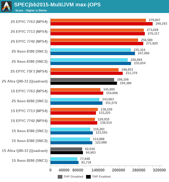
My theory here is that because of the good per-core performance of the Intel design, along with the monolithic mesh architecture, while Intel doesn’t quite catch up with AMD, it performs very well with relatively significantly fewer cores.
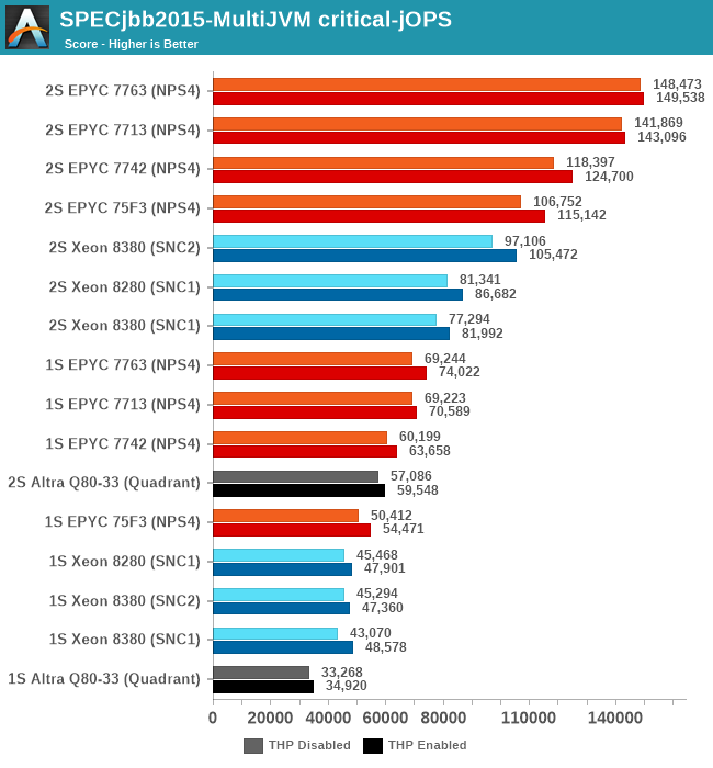
What’s really odd about the results though is that this larger increase only happens in the 2S test figures, with the 1S being unfavourable to the new Ice Lake part, losing to the 8280 in both modes. I had repeated these numbers several times to be sure they’re repeatable, and they were indeed so – as odd as that is. The 1S reduction in the critical-jOPS could be explained through the larger mesh size and larger core count of the 8380, and we did see slight regressions in core-to-core latencies. If the mesh intersection bandwidth did not increase with its size, that also could be a culprit of these figures, as the workload is hammering core-to-core transactions as well as the L3 cache of the chip.
Why the 2S figures see a bigger advantage of migrating to SNC2 could be a result of how on-chip traffic is routed, as well as the traffic flows through the UPI link blocks of the chip – at least that would be my working hypothesis.
Intel had disclosed a +62% figure for a “Java Throughput under SLA” workload they wouldn’t specify, and this does track well with our max-jOPS results. While the critical-jOPS increases seem a bit disappointing generationally, how it translates to the real world in contrast to the max-jOPS figure depends on how strict one’s SLA metrics are.


169 Comments
View All Comments
deil - Tuesday, April 6, 2021 - link
that's a lot of upgrade for intelGomez Addams - Tuesday, April 6, 2021 - link
That is a curious-looking wafer. I thought it was fake at first but then I noticed the alignment notch. Actually, I'm still not convinced it's real because I have seen lots and lots of wafers in various stages of production and I have never seen one where partial chips go all the way out to the edges. It's a waste of time to deal with those in the steppers so no one does that.JCB994 - Tuesday, April 6, 2021 - link
Periphery defects? I used to deal with those...buildup of material that would breakdown during wet processing and stream particles all over the wafer. Running partials as far out as possible helped. Nowadays...do they still use big wet benches? I have been out awhile...Gomez Addams - Tuesday, April 6, 2021 - link
Yes, they do. That's one of the systems I spent lots of time working on. Those don't look defects to me. They are just a continuation of the chip pattern.FullmetalTitan - Saturday, April 24, 2021 - link
Still the most chemical efficient tools for some etch processes. It is odd to see die prints out to the edge all around, usually at least the 'corners' are inked out/not patterned by the time it hits copper layers because printing features out that far can increase the chances of film delamination, which just leads to more defectivity. I suppose on DUV tools the extra few seconds to run those shots isn't THAT bad on non-immersion layers, but it adds up over timeArsenica - Tuesday, April 6, 2021 - link
It isn´t real if it doesn´t have DrIan bite marks./jk
ilt24 - Tuesday, April 6, 2021 - link
@Gomez AddamsI spent my entire career working in the semiconductor industry, although in IT, and I have seen many wafers from 4" to 12" and printing partial die off the edge of the wafer is quite common.
check out the pictures in these article:
https://www.anandtech.com/show/15380/i-ran-off-wit...
https://www.anandtech.com/show/9723/amd-to-spinoff...
Kamen Rider Blade - Tuesday, April 6, 2021 - link
So when are we going to hit 450 mm / 18" waffers?Are we ever going to get Hexagonal Die's to maximize possible Yields?
http://www.semiconductor-today.com/news_items/2020...
https://semiaccurate.com/2015/05/18/disco-makes-he...
They can already do that for simple LED's, but trying to bring Hexagonal IC Dies into existence is going to be exciting because there is a theoretical 62.5% increase in Manufactured Dies for a given Waffer Diameter and using Hexagonal IC Dies of a similar/identical area.
ilt24 - Tuesday, April 6, 2021 - link
@Kamen Rider Blade - "So when are we going to hit 450 mm / 18" waffers?"It seems the desire to move to EUV distracted TSMC, Samsung and Intel who are probably the only companies that were really interested in 450mm.
saratoga4 - Tuesday, April 6, 2021 - link
>So when are we going to hit 450 mm / 18" waffers?For logic, never since there is little to no advantage to larger wafers. Possibly NAND might use it, but we'll see if its even worth it there.
>Are we ever going to get Hexagonal Die's to maximize possible Yields?
Probably not for logic. With reticle sizes getting smaller in the coming nodes, it makes even less sense going forward then it did in the past, and it didn't make much sense then to begin with.