Intel 3rd Gen Xeon Scalable (Ice Lake SP) Review: Generationally Big, Competitively Small
by Andrei Frumusanu on April 6, 2021 11:00 AM EST- Posted in
- Servers
- CPUs
- Intel
- Xeon
- Enterprise
- Xeon Scalable
- Ice Lake-SP
SPEC - Per-Core Performance under Load
A metric that is actually more interesting than isolated single-thread performance, is actually per-thread performance in a fully loaded system. This actually is a measurement and benchmark figure that would greatly interest enterprises and customers which are running software or workloads that are possibly licensed on a per-core basis, or simply workloads that require a certain level of per-thread service level agreement in terms of performance.
This has been a strong-point of Intel SKUs for some time now, even when the chips wouldn’t be competitive in terms of total throughput. With the new Ice Lake SPs SKUs now more notably increasing total throughput, it’ll be interesting to see the per-thread breakdown and resulting performance:
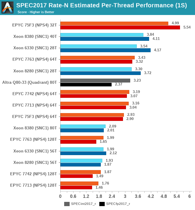
Because the total throughput generational performance increase is larger than the core count increase of the parts, this means that per-thread and per-core performance is higher with this generation. The Xeon 8380 is posting +16.3% and +10.4% per-thread performance versus the Xeon 8280 when only using one thread per core.
Interestingly, these figures are less at +8.2 and +7.4% when using both SMT threads per core. Intel has explained such an increase through the better usage of shared microarchitectural structure usage in the new Sunny Cove cores, essentially diminishing the SMT yield by improving 1/T per core performance.
Generally, Intel is extremely competitive in this benchmark metric, and while AMD easily beats them with the frequency-optimised parts, it’s an advantage that should help Intel in the SLA-centric workloads.


169 Comments
View All Comments
deil - Tuesday, April 6, 2021 - link
that's a lot of upgrade for intelGomez Addams - Tuesday, April 6, 2021 - link
That is a curious-looking wafer. I thought it was fake at first but then I noticed the alignment notch. Actually, I'm still not convinced it's real because I have seen lots and lots of wafers in various stages of production and I have never seen one where partial chips go all the way out to the edges. It's a waste of time to deal with those in the steppers so no one does that.JCB994 - Tuesday, April 6, 2021 - link
Periphery defects? I used to deal with those...buildup of material that would breakdown during wet processing and stream particles all over the wafer. Running partials as far out as possible helped. Nowadays...do they still use big wet benches? I have been out awhile...Gomez Addams - Tuesday, April 6, 2021 - link
Yes, they do. That's one of the systems I spent lots of time working on. Those don't look defects to me. They are just a continuation of the chip pattern.FullmetalTitan - Saturday, April 24, 2021 - link
Still the most chemical efficient tools for some etch processes. It is odd to see die prints out to the edge all around, usually at least the 'corners' are inked out/not patterned by the time it hits copper layers because printing features out that far can increase the chances of film delamination, which just leads to more defectivity. I suppose on DUV tools the extra few seconds to run those shots isn't THAT bad on non-immersion layers, but it adds up over timeArsenica - Tuesday, April 6, 2021 - link
It isn´t real if it doesn´t have DrIan bite marks./jk
ilt24 - Tuesday, April 6, 2021 - link
@Gomez AddamsI spent my entire career working in the semiconductor industry, although in IT, and I have seen many wafers from 4" to 12" and printing partial die off the edge of the wafer is quite common.
check out the pictures in these article:
https://www.anandtech.com/show/15380/i-ran-off-wit...
https://www.anandtech.com/show/9723/amd-to-spinoff...
Kamen Rider Blade - Tuesday, April 6, 2021 - link
So when are we going to hit 450 mm / 18" waffers?Are we ever going to get Hexagonal Die's to maximize possible Yields?
http://www.semiconductor-today.com/news_items/2020...
https://semiaccurate.com/2015/05/18/disco-makes-he...
They can already do that for simple LED's, but trying to bring Hexagonal IC Dies into existence is going to be exciting because there is a theoretical 62.5% increase in Manufactured Dies for a given Waffer Diameter and using Hexagonal IC Dies of a similar/identical area.
ilt24 - Tuesday, April 6, 2021 - link
@Kamen Rider Blade - "So when are we going to hit 450 mm / 18" waffers?"It seems the desire to move to EUV distracted TSMC, Samsung and Intel who are probably the only companies that were really interested in 450mm.
saratoga4 - Tuesday, April 6, 2021 - link
>So when are we going to hit 450 mm / 18" waffers?For logic, never since there is little to no advantage to larger wafers. Possibly NAND might use it, but we'll see if its even worth it there.
>Are we ever going to get Hexagonal Die's to maximize possible Yields?
Probably not for logic. With reticle sizes getting smaller in the coming nodes, it makes even less sense going forward then it did in the past, and it didn't make much sense then to begin with.