Intel 3rd Gen Xeon Scalable (Ice Lake SP) Review: Generationally Big, Competitively Small
by Andrei Frumusanu on April 6, 2021 11:00 AM EST- Posted in
- Servers
- CPUs
- Intel
- Xeon
- Enterprise
- Xeon Scalable
- Ice Lake-SP
Compiling LLVM, NAMD Performance
As we’re trying to rebuild our server test suite piece by piece – and there’s still a lot of work go ahead to get a good representative “real world” set of workloads, one more highly desired benchmark amongst readers was a more realistic compilation suite. Chrome and LLVM codebases being the most requested, I landed on LLVM as it’s fairly easy to set up and straightforward.
git clone https://github.com/llvm/llvm-project.gitcd llvm-projectgit checkout release/11.xmkdir ./buildcd ..mkdir llvm-project-tmpfssudo mount -t tmpfs -o size=10G,mode=1777 tmpfs ./llvm-project-tmpfscp -r llvm-project/* llvm-project-tmpfscd ./llvm-project-tmpfs/buildcmake -G Ninja \ -DLLVM_ENABLE_PROJECTS="clang;libcxx;libcxxabi;lldb;compiler-rt;lld" \ -DCMAKE_BUILD_TYPE=Release ../llvmtime cmake --build .We’re using the LLVM 11.0.0 release as the build target version, and we’re compiling Clang, libc++abi, LLDB, Compiler-RT and LLD using GCC 10.2 (self-compiled). To avoid any concerns about I/O we’re building things on a ramdisk. We’re measuring the actual build time and don’t include the configuration phase as usually in the real world that doesn’t happen repeatedly.
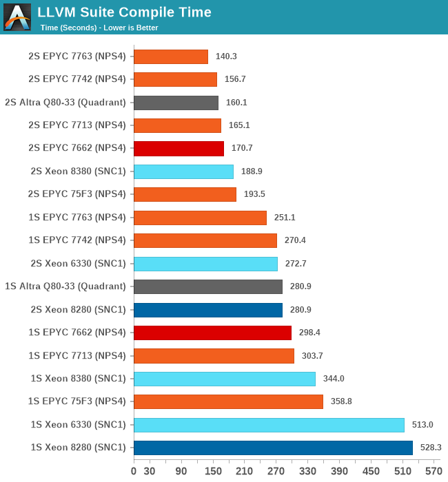
Starting off with the Xeon 8380, we’re looking at large generational improvements for the new Ice Lake SP chip. A 33-35% improvement in compile time depending on whether we’re looking at 2S or 1S figures is enough to reposition Intel’s flagship CPU in the rankings by notable amounts, finally no longer lagging behind as drastically as some of the competition.
It’s definitely not sufficient to compete with AMD and Ampere, both showcasing figures that are still 25 and 15% ahead of the Xeon 8380.
The Xeon 6330 is falling in line with where we benchmarked it in previous tests, just slightly edging out the Xeon 8280 (6258R equivalent), meaning we’re seeing minor ISO-core ISO-power generational improvements (again I have to mention that the 6330 is half the price of a 6258R).
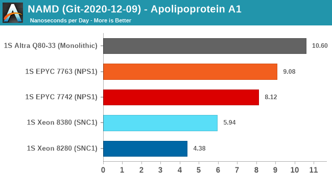
NAMD is a problem-child benchmark due to its recent addition of AVX512: the code had been contributed by Intel engineers – which isn’t exactly an issue in my view. The problem is that this is a new algorithm which has no relation to the normal code-path, which remains not as hand-optimised for AVX2, and further eyebrow raising is that it’s solely compatible with Intel’s ICC and no other compiler. That’s one level too much in terms of questionable status as a benchmark: are we benchmarking it as a general HPC-representative workload, or are we benchmarking it solely for the sake of NAMD and only NAMD performance?
We understand Intel is putting a lot of focus on these kinds of workloads that are hyper-optimised to run well extremely on Intel-only hardware, and it’s a valid optimisation path for many use-cases. I’m just questioning how representative it is of the wider market and workloads.
In any case, the GCC binaries of the test on the ApoA1 protein showcase significant performance uplifts for the Xeon 8380, showcasing a +35.6% gain. Using this apples-to-apples code path, it’s still quite behind the competition which scales the performance much higher thanks to more cores.


169 Comments
View All Comments
deil - Tuesday, April 6, 2021 - link
that's a lot of upgrade for intelGomez Addams - Tuesday, April 6, 2021 - link
That is a curious-looking wafer. I thought it was fake at first but then I noticed the alignment notch. Actually, I'm still not convinced it's real because I have seen lots and lots of wafers in various stages of production and I have never seen one where partial chips go all the way out to the edges. It's a waste of time to deal with those in the steppers so no one does that.JCB994 - Tuesday, April 6, 2021 - link
Periphery defects? I used to deal with those...buildup of material that would breakdown during wet processing and stream particles all over the wafer. Running partials as far out as possible helped. Nowadays...do they still use big wet benches? I have been out awhile...Gomez Addams - Tuesday, April 6, 2021 - link
Yes, they do. That's one of the systems I spent lots of time working on. Those don't look defects to me. They are just a continuation of the chip pattern.FullmetalTitan - Saturday, April 24, 2021 - link
Still the most chemical efficient tools for some etch processes. It is odd to see die prints out to the edge all around, usually at least the 'corners' are inked out/not patterned by the time it hits copper layers because printing features out that far can increase the chances of film delamination, which just leads to more defectivity. I suppose on DUV tools the extra few seconds to run those shots isn't THAT bad on non-immersion layers, but it adds up over timeArsenica - Tuesday, April 6, 2021 - link
It isn´t real if it doesn´t have DrIan bite marks./jk
ilt24 - Tuesday, April 6, 2021 - link
@Gomez AddamsI spent my entire career working in the semiconductor industry, although in IT, and I have seen many wafers from 4" to 12" and printing partial die off the edge of the wafer is quite common.
check out the pictures in these article:
https://www.anandtech.com/show/15380/i-ran-off-wit...
https://www.anandtech.com/show/9723/amd-to-spinoff...
Kamen Rider Blade - Tuesday, April 6, 2021 - link
So when are we going to hit 450 mm / 18" waffers?Are we ever going to get Hexagonal Die's to maximize possible Yields?
http://www.semiconductor-today.com/news_items/2020...
https://semiaccurate.com/2015/05/18/disco-makes-he...
They can already do that for simple LED's, but trying to bring Hexagonal IC Dies into existence is going to be exciting because there is a theoretical 62.5% increase in Manufactured Dies for a given Waffer Diameter and using Hexagonal IC Dies of a similar/identical area.
ilt24 - Tuesday, April 6, 2021 - link
@Kamen Rider Blade - "So when are we going to hit 450 mm / 18" waffers?"It seems the desire to move to EUV distracted TSMC, Samsung and Intel who are probably the only companies that were really interested in 450mm.
saratoga4 - Tuesday, April 6, 2021 - link
>So when are we going to hit 450 mm / 18" waffers?For logic, never since there is little to no advantage to larger wafers. Possibly NAND might use it, but we'll see if its even worth it there.
>Are we ever going to get Hexagonal Die's to maximize possible Yields?
Probably not for logic. With reticle sizes getting smaller in the coming nodes, it makes even less sense going forward then it did in the past, and it didn't make much sense then to begin with.