The Intel Xe-LP GPU Architecture Deep Dive: Building Up The Next Generation
by Ryan Smith on August 13, 2020 9:00 AM EST- Posted in
- GPUs
- Intel
- Tiger Lake
- Xe
- Xe-LP
- DG1
- Intel Arch Day 2020
- SG1
Feed the Beast: New L1 Cache & Dual Ring Buses
Shifting gears, let’s take a look at the memory subsystem for Xe-LP and how Intel will be feeding the beast that is their new GPU architecture. Among many contemporary firsts for Intel’s GPU architectures, Xe-LP will find itself in the interesting position of straddling the line between an integrated GPU and a discrete GPU. Which is to say that it has to be able to work with both Tiger Lake’s shared IMC, as well as DG1’s own dedicated memory controller.
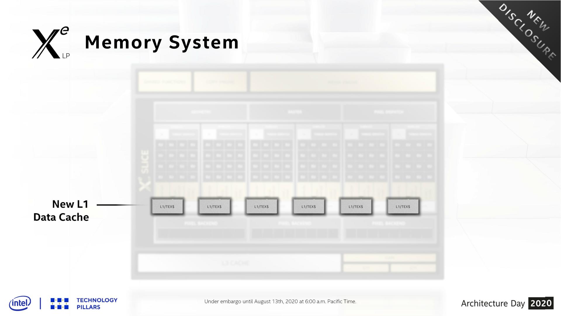
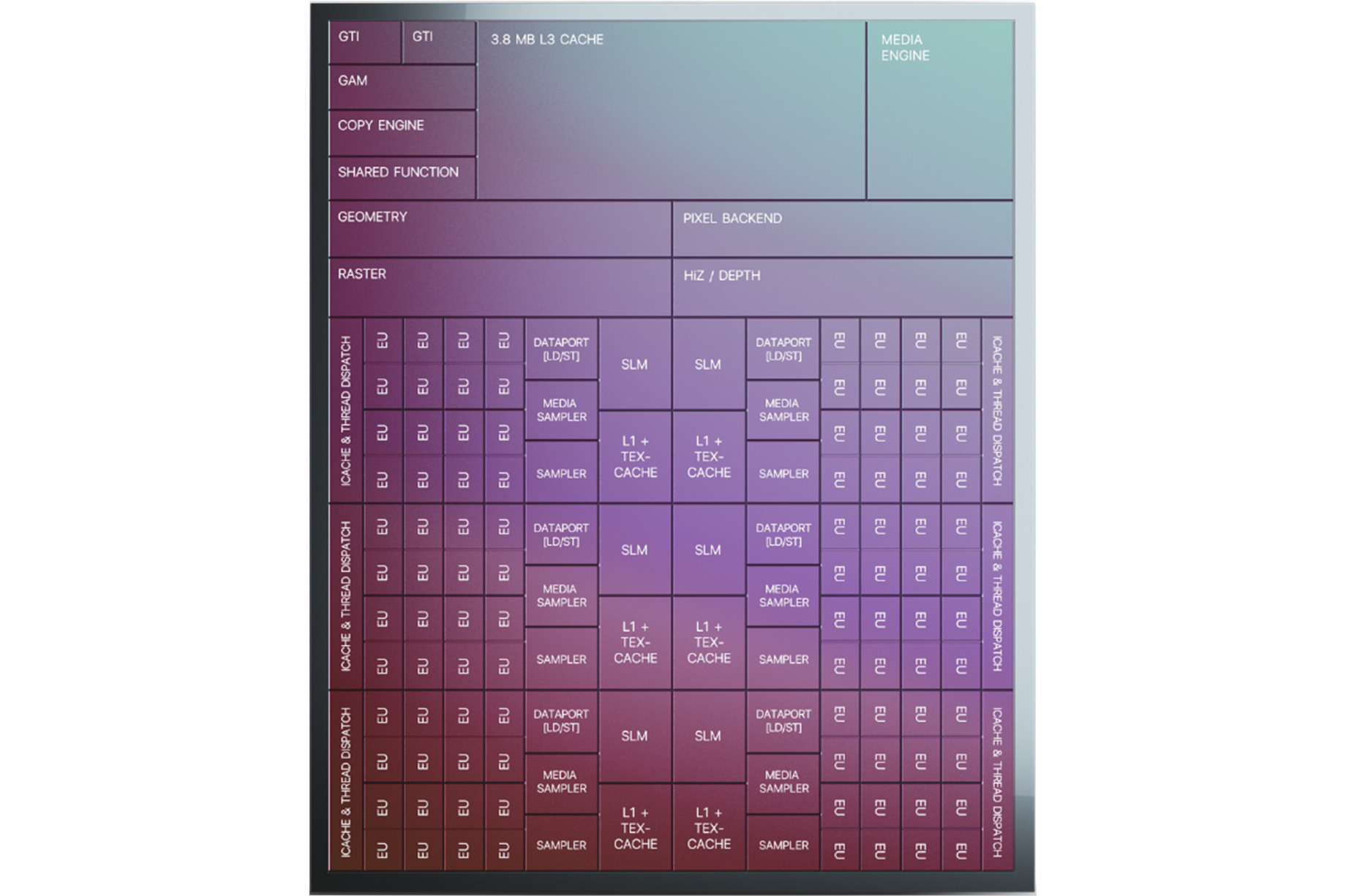
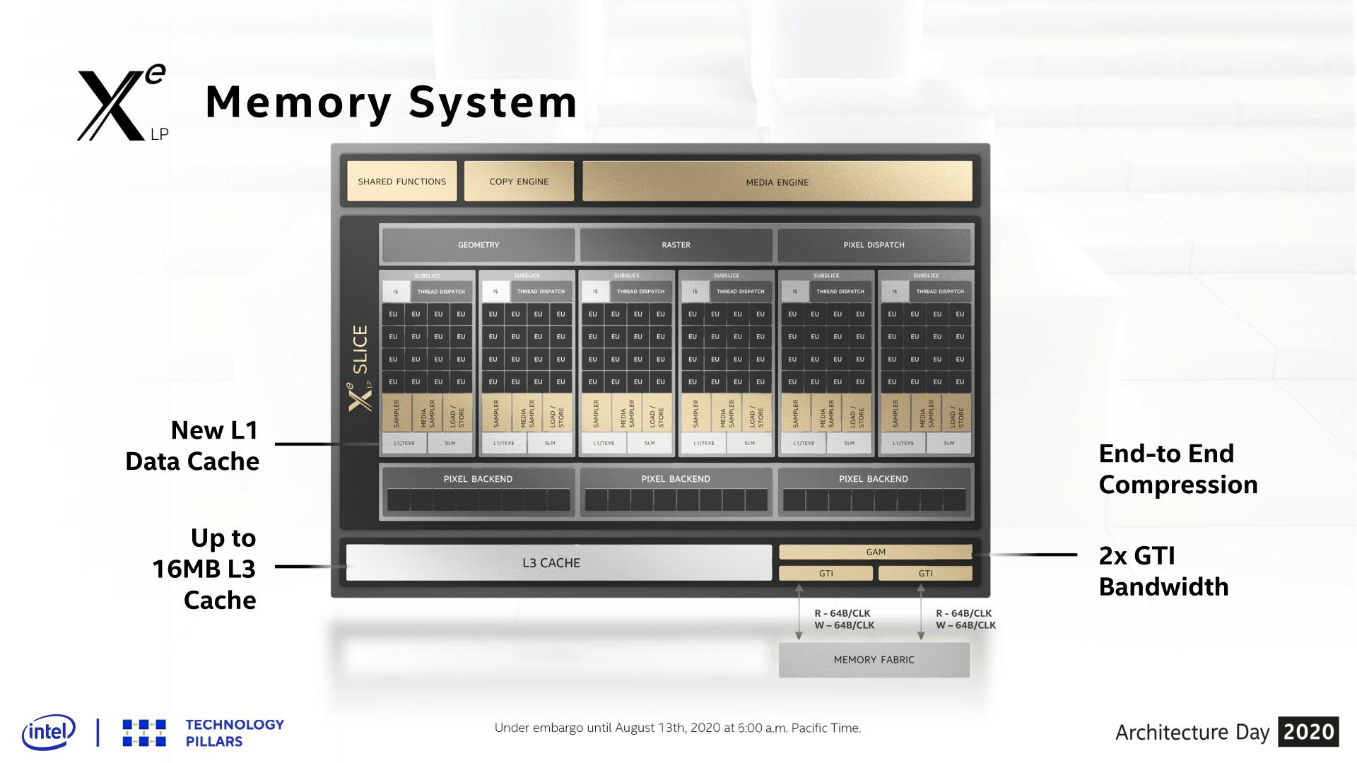
Starting with the subslices, Xe-LP introduces a new combined L1 data and texture cache. Information about this cache is limited, but Intel has confirmed that it’s a 64KB per subslice cache, and that it can be dynamically reconfigured between L1 and texture caching as necessary. According to the company, they added the L1 cache as a result of their workload analysis, and that doing so improved the performance of the load/store pipeline. Unfortunately, it’s not clear how this fits into the bigger picture with Intel’s previous subslice L2 cache, and whether that’s been replaced or still exists and is merely not on these diagrams.
The on-GPU L3 cache (not to be confused with Tiger Lake’s shared Last Level Cache) has also undergone its own upgrades, receiving both a capacity and a bandwidth boost. On the capacity front, the L3 cache can now be as large as 16MB, as opposed to just 3MB on Gen11. That said, based on Intel’s Tiger Lake disclosures, it’s clear that such a large cache isn’t coming to Intel’s SoCs; instead Tiger Lake will ship with a 3.8MB GPU L3 cache. Tiger Lake has its own LLC beyond this, which the GPU can tap into as well, so it doesn’t necessarily need quite such a large cache.
For DG1, on the other hand, the GPU’s L3 cache is the last caching level, so a larger cache makes practical sense there. To that end I wouldn’t be surprised if that’s exactly what we see on DG1: a 16MB L3 cache. Though Intel has reiterated that this is an architectural presentation and not a product presentation, so it may very well be that they aren’t outfitting any Xe-LP GPUs with a max size L3 cache.
This larger L3 cache is also faster than Gen11’s L3, with Intel doubling the transfer size. Xe-LP’s L3 cache can now transfer 128 bytes/clock, which for a theoretical 1.6GHz chip would give it over 190GB/sec of internal L3 bandwidth. This upgrade is important for feeding the ROPs and other parts of the GPU, and goes hand-in-hand with Intel’s goal to double GPU performance, which means they need to feed the beast a lot more data in the process. Plus this change also keeps the L3 cache aligned with what the new dual ringbus can do.
One of the more enigmatic changes for Tiger Lake, the SoC has added a second, seemingly identical ringbus to the chip, creating a second loop that connects the four CPU cores and the iGPU to the integrated memory controller. As a consequence of this, the iGPU now needs two Graphics Technology Interface (GTI) ports to create the two ringbus stops.
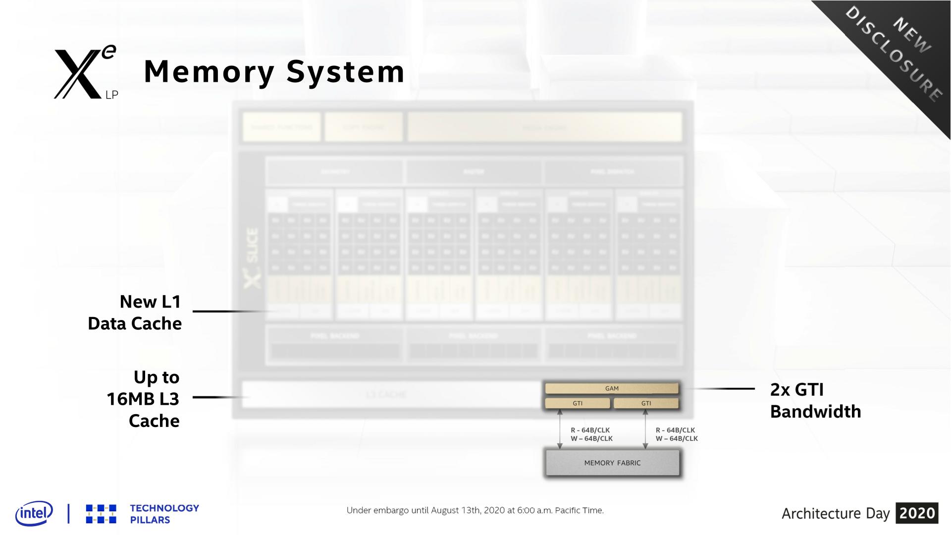
The big benefit of this change is that, all other aspects held equal, this doubles the amount of bandwidth between the GPU and the IMC on Tiger Lake. So instead of only being able to transfer 64B/clock up and down, Xe-LP on Tiger Lake can send two 64B requests (for a total of 128B/clock) using the two ringbuses.
Given that at this juncture the iGPU has become the largest consumer of bandwidth on an Intel SoC, I strongly suspect that the second ringbus has been added primarily for the iGPU’s benefit. Unfortunately this isn’t something we can directly math out, as the ringbus having its own clock domain complicates matters a bit, so it’s not clear if 1 ringbus can even match the memory bandwidth of a Tiger Lake chip with LPDDR5-5200. But even if it can, the an even higher performing GPU like Xe-LP is no doubt putting a good deal of pressure on Intel’s SoC memory subsystem.
Meanwhile this also gives us a very strong hint that DG1 will utilize a 128-bit memory bus for its dedicated VRAM. The 2x64B backend could very easily be hooked up to a 128-bit memory controller, instead of the two 64B ringbuses. This would also ensure that DG1 gets as much or more memory bandwidth than Tiger Lake – and with the bonus of not having to share it with other parts of the system.
Finally, even with the significant bandwidth improvements underneath, Intel has also been working to reduce their bandwidth consumption. Xe-LP ships with updated versions of their color and depth compression algorithms, which although Intel isn’t providing specific figures for it, any improvements here will directly translate into reduced memory traffic. Meanwhile the company is also extending this compression functionality to the media and display interfaces, which means that image data can stay compressed whenever it’s being moved between the graphics engine, the media engine, and the display.


33 Comments
View All Comments
mode_13h - Thursday, August 13, 2020 - link
As always, thanks for the deep coverage.Not finished reading, but I already have one complaint:
> Gen11’s smallest wavefront width is 8 threads wide (SIMD8), so it can take multiple clock cycles to execute a single wavefront, with Intel interleaving multiple threads as a form of latency hiding.
Wow. Mixing 2 different definitions of "thread" in the same sentence? Please don't.
Last I checked Nvidia is the only one talking about SIMD lanes as if they're threads. In Intel's Gen 9 whitepaper, it uses "threads" in a manner equivalent to CPU threads, and they talk about SIMD lanes as SIMD lanes.
And speaking of Gen 9, they claim it has 7-way SMT. Did they ever specify this, for Gen 11? I don't recall seeing it in their Gen 11 whitepaper, which went into significantly less detail on the EUs than previous whitepapers.
mode_13h - Thursday, August 13, 2020 - link
I guess your article could be self-consistent by replacing the second use of "thread" in that quoted sentence with "wavefront"?Although, "wavefront" is an AMD term (Nvidia calls them "Warps"). However, Intel's slides suggest they still call them "threads".
Ryan Smith - Thursday, August 13, 2020 - link
"I guess your article could be self-consistent by replacing the second use of "thread" in that quoted sentence with "wavefront"?"You are correct sir! That was supposed to be "wavefront".
And Intel tends to use "wave" in its literature, though I prefer to collapse it down to just wavefront to keep things reasonably consistent. We don't need 2 nearly-identical terms for the same thing.
mode_13h - Thursday, August 13, 2020 - link
Cool. Thanks for the reply!BTW, I don't mind the term "wavefront" - I said that more to point it out to those who might not know.
mode_13h - Thursday, August 13, 2020 - link
IMO, the reason Nvidia has long called their Warp elements "threads" is so they can claim that each SIMD lane is a "core", to make their GPUs *sound* more impressive.Since Volta finally fixed their per-lane IP register (which is basically just a fancy form of branch predication), there's almost a touch of truth in that characterization, and I'd finally agree that their ISA is more than just a straight-forward combination of SIMD + SMT.
xenol - Thursday, August 13, 2020 - link
AMD feels more confusing. Their base unit is a "stream processor" which seems to suggest something larger than it really is. But a group of stream processors is called a Compute Unit, which that seems to suggest something smaller than it really is.Though looking at some of the programming literature for GPUs, I can see where the "thread" terminology comes from. So this looks more like a problem of someone coming up with their own language instead of the industry coming together to standardize on it. However, given that NVIDIA, AMD, and Intel have their own way of doing things, it may not be possible to do that and for the sake of clarity, having their own terminology is more or less correct.
mode_13h - Thursday, August 13, 2020 - link
Since Nvidia's Fermi and AMD's GCN, their architectures basically amount to SIMD + SMT. I'm not sure exactly when Intel added SMT.Anyway, I wouldn't characterize their architectures as fundamentally different. Intel is traditionally the most distinct, among the three.
jim bone - Friday, August 14, 2020 - link
recent editions of Hennessy and Patterson have a nice table mapping the CPU terminology to nvidia’s GPU terminology:https://books.google.ca/books?id=cM8mDwAAQBAJ&...
jim bone - Friday, August 14, 2020 - link
and yes for reasons nvidia calls a vertical slice of simd instructions a threadkpx86 - Thursday, August 13, 2020 - link
I believe the SW libraries like DirectX and OpenGL use threads this way.From MSFT website: The maximum number of threads is limited to D3D11_CS_4_X_THREAD_GROUP_MAX_THREADS_PER_GROUP (768) per group.