Intel’s 11th Gen Core Tiger Lake SoC Detailed: SuperFin, Willow Cove and Xe-LP
by Dr. Ian Cutress on August 13, 2020 9:01 AM EST- Posted in
- CPUs
- Intel
- SoCs
- Tiger Lake
- 10+
- Xe-LP
- Willow Cove
- Intel Arch Day 2020
- SuperFin
- 10SF
Tiger Lake IO and Power
As part of Tiger Lake, other enhancements have been made to the chip outside of the traditional CPU/GPU components. In this article, as they directly impact core performance, we’ve already discussed improvements to the fabric, enabling a doubling of bandwidth with the dual bidirectional ring design, and the new LPDDR5-5400 support on the memory controller – go back a couple of pages to find information on these.
PCIe 4.0 Support
We lightly touched upon it in the graphics section, but the four core Tiger Lake processor will be the first mobile processor to support PCIe 4.0 directly from the CPU. Intel hasn’t specifically stated how many lanes of PCIe 4.0 the processor will support, which is kind of frustrating at this time, but they have made it clear that they have not experienced a power penalty moving from PCIe 3.0 in Ice Lake to PCIe 4.0 in Tiger Lake.
As it stands, Intel expects the PCIe 4.0 lanes to be used in these mobile processors primarily for PCIe 4.0 storage, however given the status of the current PCIe 4.0 NVMe SSDs on the market today and the high power requirements of the Phison E16 controller (~8W), we might have to wait a bit for other controllers to come in volume.
Intel did state that the quantity of PCIe 4.0 lanes did have a direct correlation with the CPU count and the power of the chip, but refused to state what the scaling is. Based on comments made by Intel during the Architecture Day, such as Tiger Lake supporting 24 MiB of L3 cache which would require an 8-core CPU, we suspect that a full 16 PCIe 4.0 lane version (or more?) to align with that product instead. That would mean the 4-core Tiger Lake version would be more akin to an 8-lane processor, which would gel with what we’ve seen with other mobile processors in the past.
However, there is part of me that suspects that this processor has only four PCIe 4.0 lanes. Intel’s quote about remaining iso-power between Ice Lake (PCIe 3.0 x8) and Tiger Lake on PCIe 4.0 might actually be that tradeoff – moving down to four lanes keeps that iso-power. Even with four PCIe 4.0 lanes, that’s still enough for a discrete Thunderbolt graphics card and a super-fast NVMe SSD, or dual NVMe 4.0 x2 drives. The higher data rates on PCIe 4.0 do require more power per lane, assuming an iso-process, as we’ve presumed with other products, but there are always silicon improvements that might help with that.
Update: Another element to support the PCIe 4.0 x4 theory – in multiple places during Architecture Day, Intel states that devices accessing memory over PCIe will have ‘8 GB/s bandwidth. Each PCIe 4.0 x1 link is approx. ~2 GB/sec, which would imply there is only four.
Gaussian and Neural Accelerator 2.0 (GNA)
One of the accelerators that Intel offered in Ice Lake was the GNA - a simple low power inferencing engine that enables the system to offload basic analysis or workloads such as noise reduction for calls or voice recording. In a previous guise, the GNA built upon the Gaussian Mixture Model, which we believe was IP dedicated to accelerating Microsoft’s Cortana in voice recognition. With Tiger Lake, we now get GNA 2.0.

No specifics were necessarily given as to what has changed this time around, aside from having the benefits of the 10SF process technology. Intel did quote some handy numbers though, stating that GNA 2.0 can perform 1 GigaOP at 1 milliwatt, and this can scale linearly up to 38 GigaOPs for 38 milliwatts. Intel never released similar performance/efficiency numbers for Ice Lake, stating only that GNA 2.0 is ‘enhanced’ for Tiger Lake.
Display and Image Processing Unit
We’ve covered the Display aspects of the Tiger Lake in the graphics section, but to reiterate, there are four 4K display pipelines: DP1.4, HDMI 2.0, Thunderbolt 4, and USB4 Type-C can be used simultaneously. The display engine also supports HDR10, 12-bit BT2020 color, Adaptive Sync, and support for monitors up to 360 Hz, and Intel states that the display engine can support up to 64 GB/s to memory, suggesting there is some overhead or bottleneck compared to the 86.4 GB/s supported by LPDDR5-5400. Tiger Lake also supports direct-to-memory data transfer for the display engine, bypassing the CPU – a feature first introduced with Skylake.
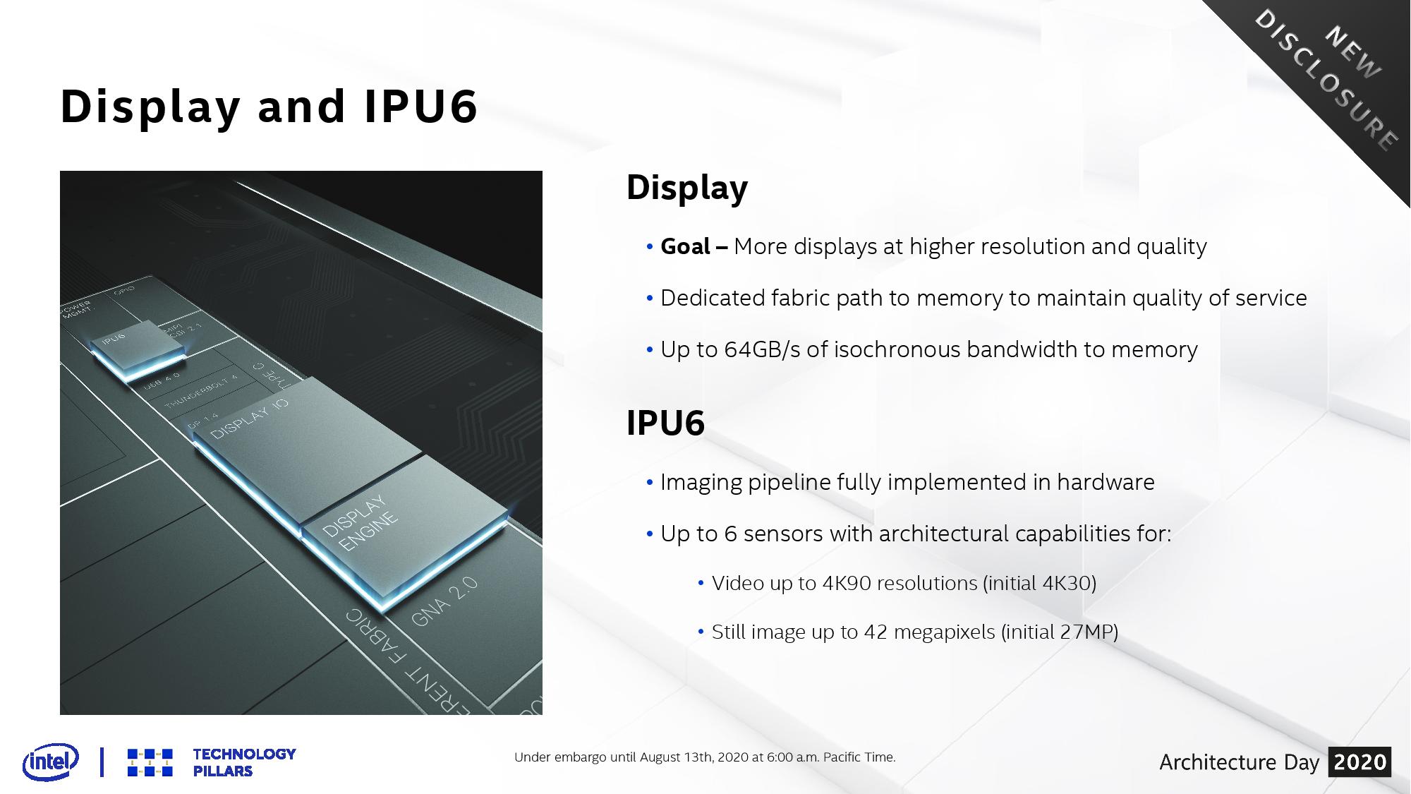
For the image processing unit, Intel has used the 10SF transistor budget to increase the size of its imagine pipelines in hardware. There is still support for six cameras, the same as Ice Lake, but the Tiger Lake silicon will eventually be capable of 4K90 video and 42 MP imaging support. Notice the ‘will eventually be capable’ in that last sentence – Intel has specified that this four core Tiger Lake will only support 4K30 and 27MP for video and imaging respectively. It wasn’t clarified at the time why there was this discrepancy and what it means, but our best guess is one of two things: the larger 8-core version of Tiger Lake (the one with the 24 MiB L3 cache that Intel kept talking about) will have the full support, or the full support can only be enabled with faster memory such as LPDDR5-5400, which won’t be available until mid-way through Tiger Lake’s product cycle.
Thunderbolt 4
Tiger Lake will be Intel’s first deployment of Thunderbolt 4 hardware, and the company will follow up with TB4 controllers for non-TGL systems later this year. TB4 is a superset of the USB4 standard, and thus Tiger Lake will also support USB 4. The way the Tiger Lake chip is built, two Thunderbolt 4 ports will be supported on each side of the laptop, and each port will support the full 40 Gb/s bandwidth. In order to qualify for next generation Athena specifications, one of those will need to be a quick-charging port.
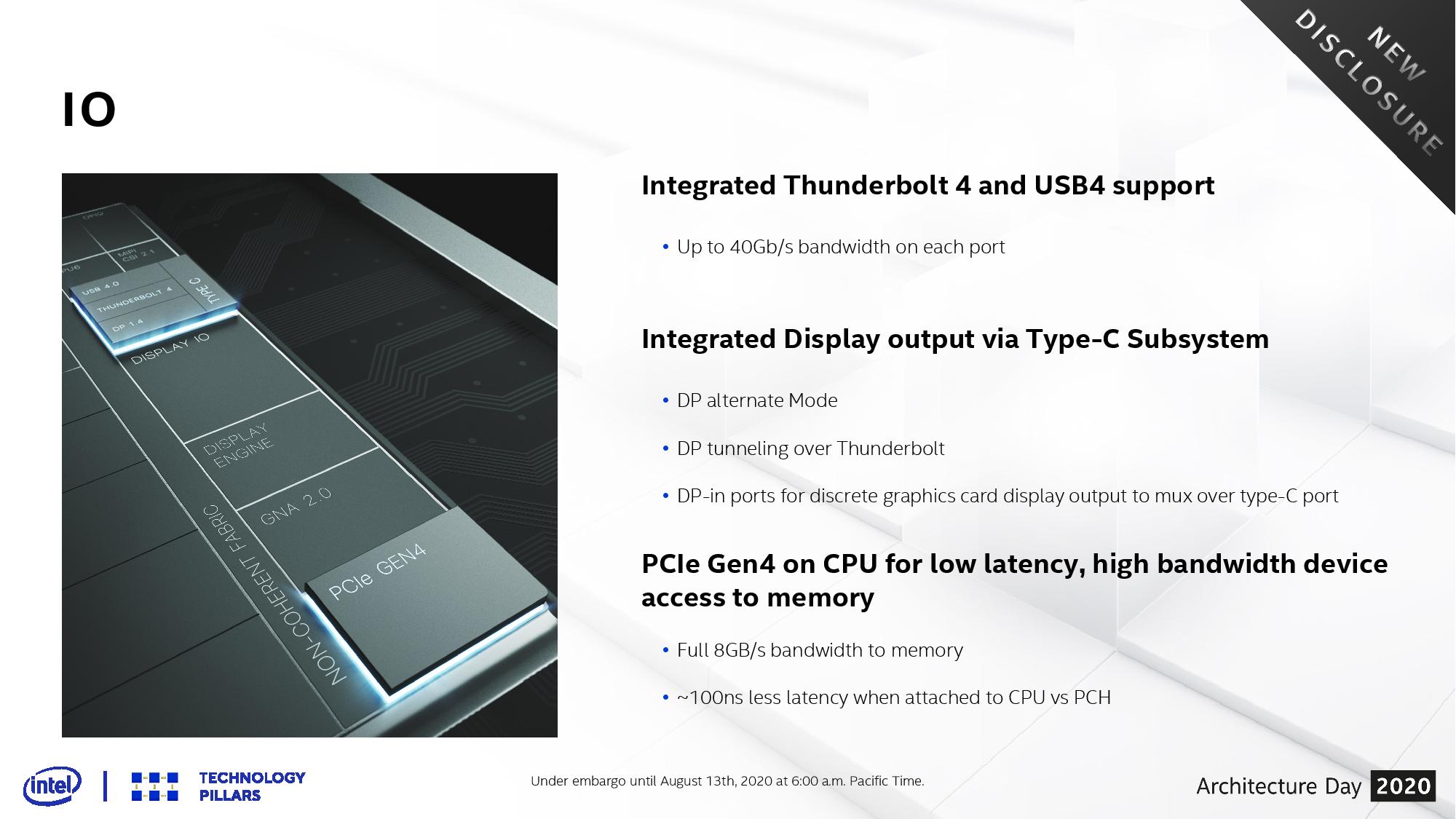
We covered Thunderbolt 4 a few weeks ago, as Intel wanted to discuss TB4 ahead of the Tiger Lake launch. One of the key requirements for TB4 certification is that the processor must support some form of DMA write protection to prevent physical attacks. Intel does this through its processors supporting VT-d instructions, and when TB4 controllers come out, other processor vendors will have to enable similar technologies. Another TB4 certification requirement is going to be supporting wake-from-sleep through any TB4 device, such as a dock.
Power Management and Frequency/Voltage Scaling
One of the most important drivers with mobile processors is idle and sleep power – the more parts of the chip that can be put into a low power state when not in use, the better the battery life.
At a high level this means that if a laptop is playing a video, on the CPU we have the display engine is on and the video decode on, but most/all of the cores are in a low power state or a deep sleep mode, and the graphics are essentially tuned off, and the fabric is powered down as much as possible. As we move to denser process nodes with bigger transistor budgets, more of those transistors are being used to create individual power and frequency domains in order to manage how a processor deals with sub-dividing its parts for low powered modes.
On top of that, logic needs to be applied to manage all the different domains, and it needs to be designed such that when the parts that are turned off are needed again, they can be powered up with no noticeable delay to the end user.
With every generation of laptop product, both Intel and AMD continually introduce new features and better control over the different compute and interconnect blocks within mobile processors where it matters the most. For Tiger Lake, Intel has an updated its autonomous dynamic voltage/frequency scaling (DVFS) algorithms to take into account bandwidth requirements for a given workload.
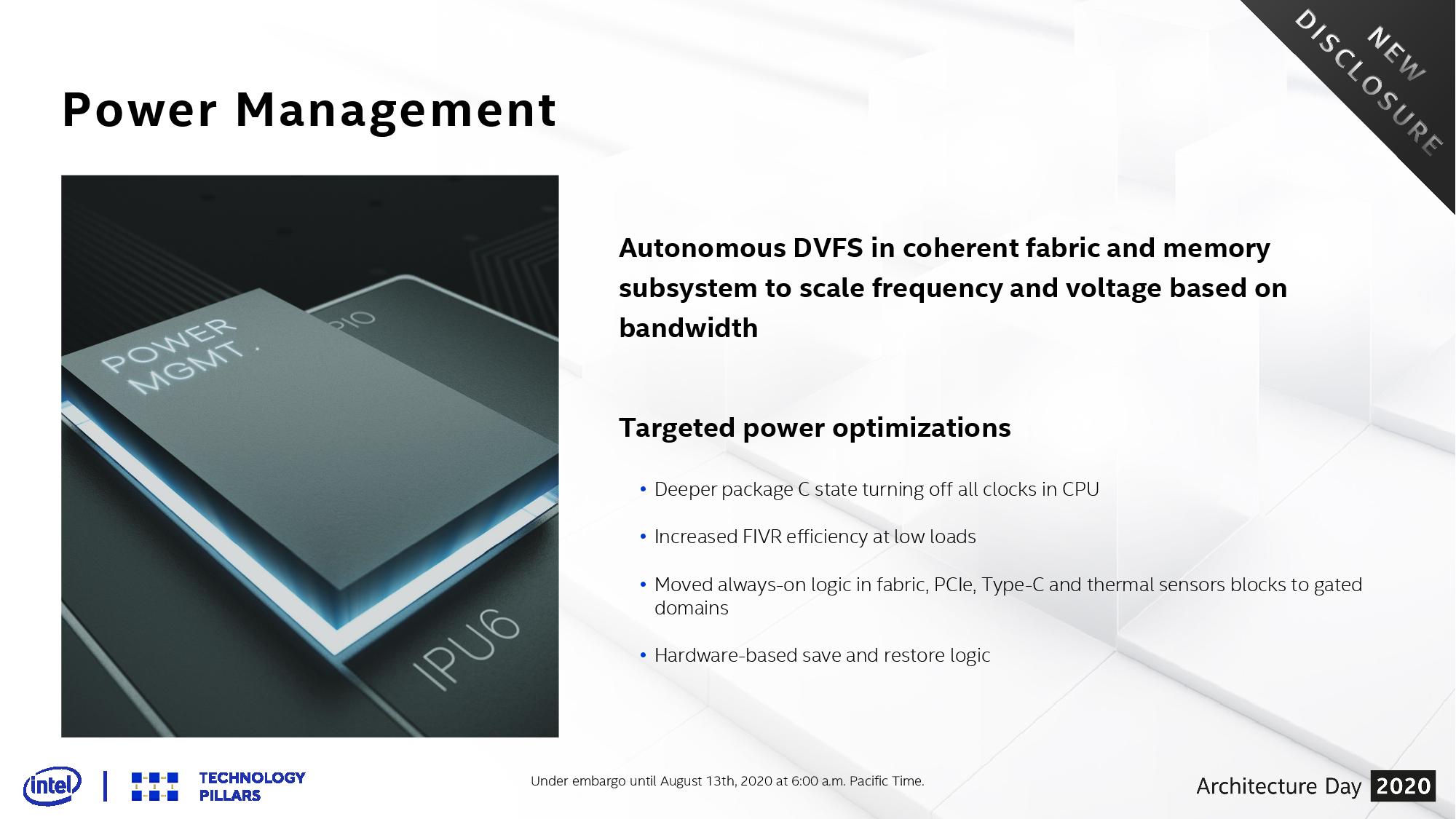
This is done on top of other power optimizations at an SoC level, such as even better clock gating for the CPU cores and better voltage regulator efficiency for the integrated regulators. With Tiger Lake, even the PCIe, USB and thermal sensors now occupy their own domains for sleep states. When a component needs to be put in sleep, if it contains important data that often needs to be ‘saved’ somewhere for when it is restored: Intel now has improved hardware-based save and restore logic for this purpose, going beyond Ice Lake’s offerings. Exactly how much change has been made hasn’t been quantified, but the idea is that all these small adjustments will add up over time.


71 Comments
View All Comments
Quantumz0d - Thursday, August 13, 2020 - link
"The others not mentioned will be split between 7nm and external fabs. More on that info in a separate article"So that means they are going for external fab really. Damn. What a shame. I wonder if that's the CPU or this GPU. Anything is a shame on Intel and that beancounter Bob.
IanCutress - Thursday, August 13, 2020 - link
That's referring to the other tiles of Ponte Vecchio. There are 4. We covered 2.Eliadbu - Thursday, August 13, 2020 - link
Shame is when you don't acknowledge your problems and how they might limit you. Going with external fabs allows the company to be competitive where it needs the most. But they sure need a long term strategy and and make critical decisions like which processes they would utilize earlier.Kangal - Thursday, August 13, 2020 - link
It's only GPU.And it's only the Xe-HP (ergo Discreet GPU) variant.
It seems to imply that is only on the 10SFE "enhanced" variant. Basically using TSMC 7nm process for the higher memory and connector chips, named as "Rambo Cache" and "Xe Link". And that's targeting the server market and high-end desktops (ie think Nvidia Titan).
Seems like Intel realise how embarrassing it is to ask for their competitors wafers for their main product, so instead they're taking a half-measure and using it for the GPU only. That way they get to save face and say "well, AMD and Nvidia do it too". Also it seems they couldn't get any good prices, which is why only some chips are made on the 7nm, and rest are made in-house on 10nm. Overall, this is Intel playing hard to catch up to TSMC's 7nm and AMD's Zen2 and AMD's Vega. That's why the whole thing is difficult to understand, as it is purposely obfuscated. Yet these will only ship in (late) 2021, whereas the competition is posied to actually leap ahead in 2020 to +7nm TSMC, Zen3, RDNA2. And when Intel arrives, they might even be facing off against 5nm and a Zen3+ refresh. Just to put things into perspective.
tipoo - Thursday, August 13, 2020 - link
This reads quite promising. Great writeup."A few angstroms thick" it's hard to even think about the scale of this stuff, that's 0.1 nanometres or 100 picometres. How far from atomic bonding limits?
DrJackMiller - Thursday, August 13, 2020 - link
It's pretty damn close, but that depends on the bond :-). For a perhaps more human comparison, that of O-O in Oxygen is 1.208 Å; and in C=O bonds (e.g. in CO2) it's around 1.16 Å.vortmax2 - Friday, August 14, 2020 - link
Would love to see an article here of the next 10-20 years of processors as we enter deeper into the atomic scale. What the next big breakthrough?jospoortvliet - Saturday, August 15, 2020 - link
Less promising is that they went for a four cores design again. With AMD pushing the desktop to 8 with the first Zen you would think they would realize amd would pull the same when going mobile and prepare for it... so is this arrogance thinking their cores are so much better or they control the market? Lack of strategic insight? Or inability to work out things for the yield and cost math?Spunjji - Monday, August 17, 2020 - link
If these cores are as good as they're claiming they are, there will be a legitimate dilemma choosing between 4 Very Fast cores and 8 Really Quite Fast cores.I'd wager that yields are 80% to blame and power is the rest - they have an 8-core Tiger in the works, but it's a 35/45W part and there's nothing firm about a release date yet.
none12345 - Tuesday, August 18, 2020 - link
Depends on the atoms, but for reference how about silicon."Silicon has the diamond cubic crystal structure with a lattice parameter of 0.543 nm. The nearest neighbor distance is 0.235 nm."
Diatomic hydrogen is the smallest molecule with a bond length of 0.74 angstrom.
Bond length is typically 1-2 angstrom.
"Intel states that this is an industry first/leading design, enabled through careful deposition of new Hi-K materials in thin layers, smaller than 0.1nm, to form a superlattice between two or more material types."
Unless im missing something, the above statement does not make any sense to me. thin layers of atoms less then the average bond length between atoms is nonsensical.