Intel’s 11th Gen Core Tiger Lake SoC Detailed: SuperFin, Willow Cove and Xe-LP
by Dr. Ian Cutress on August 13, 2020 9:01 AM EST- Posted in
- CPUs
- Intel
- SoCs
- Tiger Lake
- 10+
- Xe-LP
- Willow Cove
- Intel Arch Day 2020
- SuperFin
- 10SF
What is Xe-LP?
A big part of the Tiger Lake/Ice Lake comparison will be the performance difference in graphics. Where Ice Lake has 64 Execution Units of Gen11 graphics, Tiger Lake has 96 Execution Units but of the new Xe-LP architecture. On top of that, there’s the new SuperFin transistor stack that promises to drive frequencies (and power windows) a lot higher, making Tiger Lake more scalable than before.
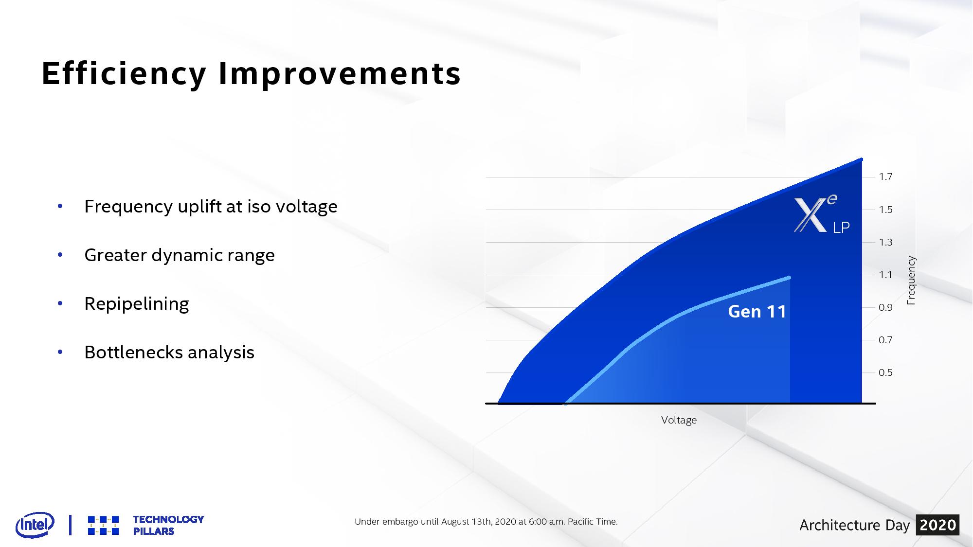
Straight off the bat Intel’s graphs are showing that at the same voltage, where Ice Lake Gen11 achieves 1100 MHz, the new Xe-LP graphics will get to ~1650 MHz, a raw +50% increase. That means at Ice Lake’s peak power, we should expect Tiger Lake to perform at a minimum 2.25x better. Expanding beyond that, the peak for Tiger Lake seems to be in the 1800 MHz range, ultimately giving a minimum 2.45x more performance over Ice Lake. This is before we even start talking about the fundamental differences in the Xe-LP architecture compared to Gen11.
Intel is promoting Xe-LP as operating at 2x the performance of Gen11, so even though these numbers might easily suggest a 2.25x uplift before taking into account the architecture, it will ultimately depend on how the graphics is used.
Gen11 vs Xe-LP
For a more in-depth look into Intel’s Xe graphics portfolio, including HP, HPC, and the new gaming architecture HPG, Ryan has written an article covering Xe in greater detail. In this article, we’ll cover the basics.
In the Ice Lake Gen11 graphics system, each one of the 64 execution units consisted of two four-wide ALUs, one set of four for FP/INT, and the other set of four for FP/Extended Math. 16 of these execution units would form a sub-slide within Gen11.
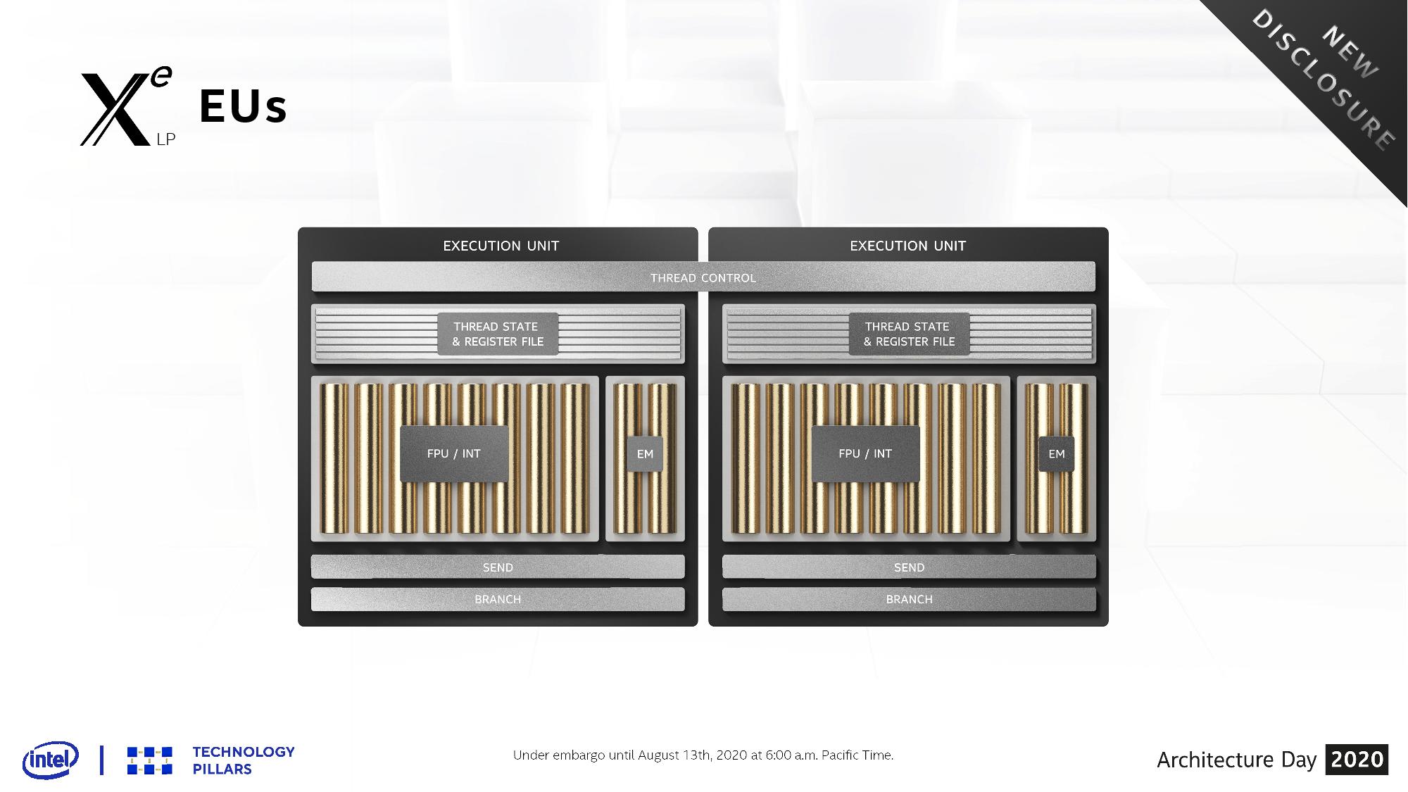
For Xe-LP, that 4+4 per execution unit has been rebalanced for this target market. There are now 10 ALUs per execution unit, but in an 8+2 configuration. The 8 ALUs support 2xINT16 and INT32 data types, but also with new DP4a instructions can accelerate INT8 inference workloads. The new execution units also now work in pairs – two EUs will share a single thread control block to help assist with coordinated workload dispatch.
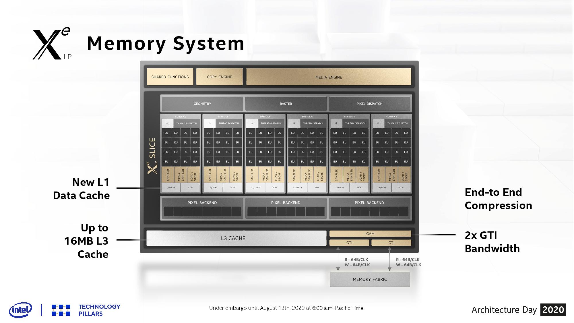
As with ICL, 16 of the EUs now form a sub-slice with the graphics, and slices are added in the SoC as performance is needed. What is new in Tiger Lake is that each sub-slice now has its own L1 data and texture cache, and the pixel backend runs 8 pixels/clock per two sub-slices.
Overall the graphics system can support 1536 FLOP/clock, with the samplers at 48 Tex/clock per sub-slice and a total of 24 pixel/clock in the back-end. LP in Tiger Lake has 16 MiB of its own L3 cache, separate from the rest of the L3 cache in the chip, and the interface to the memory fabric is doubled, supporting 2x64B/clock reads or writes or a combination of both.
Exact performance numbers for Xe-LP in Tiger Lake are going to be a question mark until we get closer to launch. Intel has stated that the discrete graphics version of LP, known as DG1, is due out later this year.
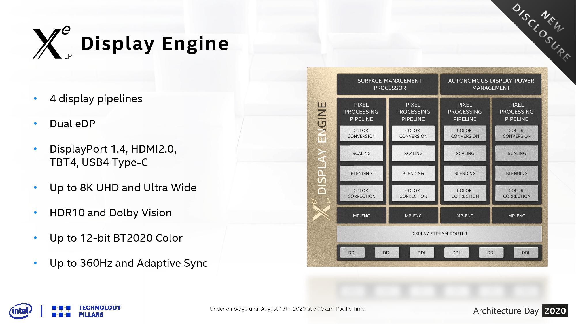
Xe-LP Media and Display
The other question on Tiger Lake on graphics will be the media and display support. Tiger Lake will be Intel’s first official support for the AV1 codec in decode mode, and Intel has also doubled its encode/decode throughput for other popular codecs. This means a full hardware-based 12-bit video pipeline for HDR and 8K60 playback support.
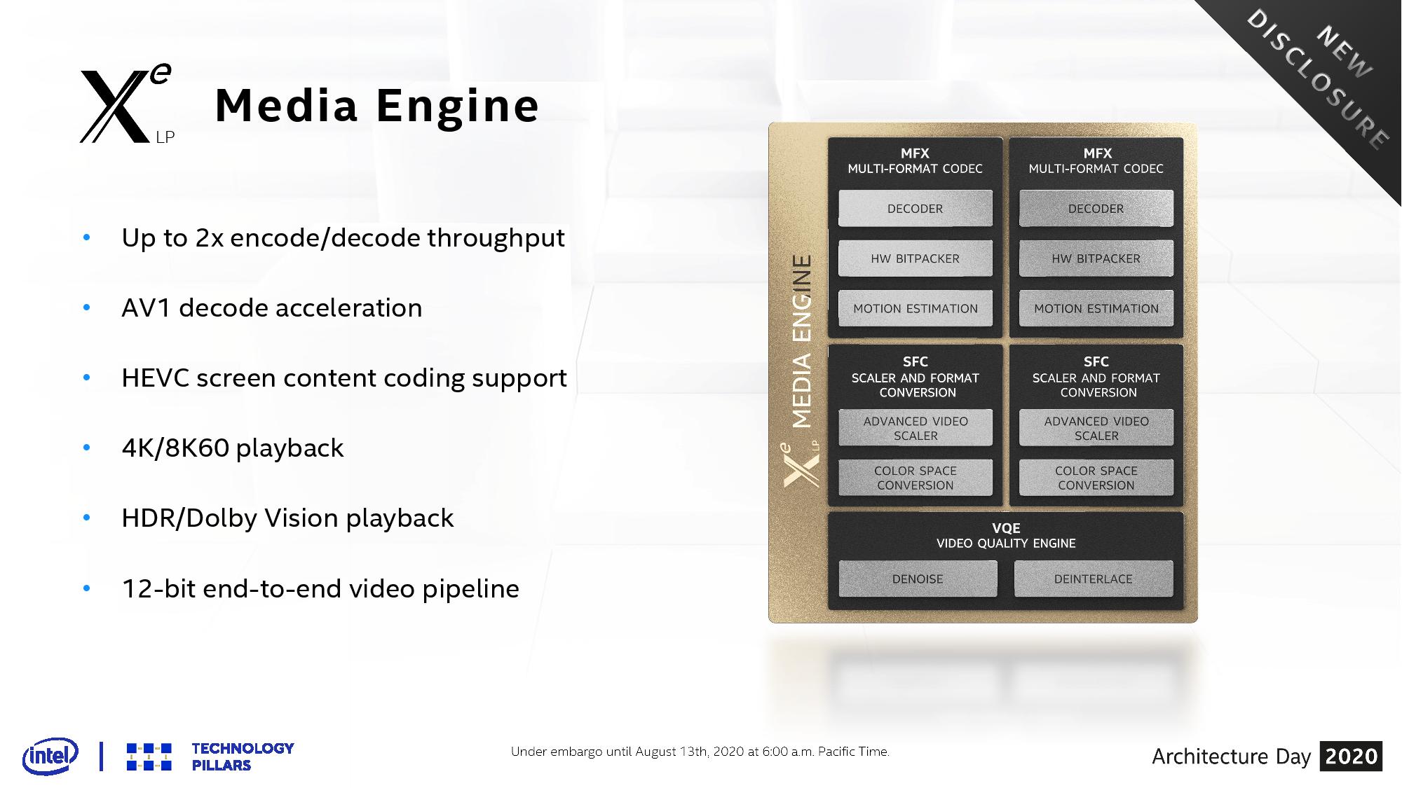
Display Support for Tiger Lake is also extended with four 4K display pipelines. Connections over DP1.4, HDMI 2.0, Thunderbolt 4, and USB4 Type-C simultaneously is how Intel expects users to operate if all four outputs are needed at once. The display engine also supports HDR10, 12-bit BT2020 color, Adaptive Sync, and support for monitors up to 360 Hz.
External Graphics and Hybrid Support
One of the interesting questions we posted to Intel during Architecture Day was surrounding how Xe-LP will operate in the presence of additional graphics, and potentially paired with a discrete version of LP later in the year. Unfortunately there seemed to be some confusion between the definitions of ‘hybrid’ graphics vs ‘switchable’ graphics, so we got that cleared up in time for the article.
At present, Intel expects almost all Tiger Lake solutions to run in devices where there is no discrete graphics solution – only the integrated graphics is provided as the primary compute for gaming and acceleration. However, Tiger Lake will support switchable graphics solutions with Xe-LP discrete graphics. Intel did not state if this was discrete graphics with respect to a built LP chip or an external discrete graphics solution through Thunderbolt.
Due to Tiger Lake’s PCIe 4.0 support and Thunderbolt 4 support, depending on how an exact Tiger Lake system is configured, Intel expects that any discrete graphics solution will operate at a lower latency, mostly due to the fact that the PCIe 4.0 lanes will be directly attached to the CPU, rather than a chipset. Intel quoted ~100 nanosecond lower latency. They also stated an 8 GB/s bandwidth to main memory, which seemed a bit low?
On the topic of hybrid graphics, where the integrated graphics and an Xe-LP discrete solution could work in tandem on the same rendering task, Intel stated that there is no plan to support a Multi-GPU solution of this configuration.


71 Comments
View All Comments
Quantumz0d - Thursday, August 13, 2020 - link
"The others not mentioned will be split between 7nm and external fabs. More on that info in a separate article"So that means they are going for external fab really. Damn. What a shame. I wonder if that's the CPU or this GPU. Anything is a shame on Intel and that beancounter Bob.
IanCutress - Thursday, August 13, 2020 - link
That's referring to the other tiles of Ponte Vecchio. There are 4. We covered 2.Eliadbu - Thursday, August 13, 2020 - link
Shame is when you don't acknowledge your problems and how they might limit you. Going with external fabs allows the company to be competitive where it needs the most. But they sure need a long term strategy and and make critical decisions like which processes they would utilize earlier.Kangal - Thursday, August 13, 2020 - link
It's only GPU.And it's only the Xe-HP (ergo Discreet GPU) variant.
It seems to imply that is only on the 10SFE "enhanced" variant. Basically using TSMC 7nm process for the higher memory and connector chips, named as "Rambo Cache" and "Xe Link". And that's targeting the server market and high-end desktops (ie think Nvidia Titan).
Seems like Intel realise how embarrassing it is to ask for their competitors wafers for their main product, so instead they're taking a half-measure and using it for the GPU only. That way they get to save face and say "well, AMD and Nvidia do it too". Also it seems they couldn't get any good prices, which is why only some chips are made on the 7nm, and rest are made in-house on 10nm. Overall, this is Intel playing hard to catch up to TSMC's 7nm and AMD's Zen2 and AMD's Vega. That's why the whole thing is difficult to understand, as it is purposely obfuscated. Yet these will only ship in (late) 2021, whereas the competition is posied to actually leap ahead in 2020 to +7nm TSMC, Zen3, RDNA2. And when Intel arrives, they might even be facing off against 5nm and a Zen3+ refresh. Just to put things into perspective.
tipoo - Thursday, August 13, 2020 - link
This reads quite promising. Great writeup."A few angstroms thick" it's hard to even think about the scale of this stuff, that's 0.1 nanometres or 100 picometres. How far from atomic bonding limits?
DrJackMiller - Thursday, August 13, 2020 - link
It's pretty damn close, but that depends on the bond :-). For a perhaps more human comparison, that of O-O in Oxygen is 1.208 Å; and in C=O bonds (e.g. in CO2) it's around 1.16 Å.vortmax2 - Friday, August 14, 2020 - link
Would love to see an article here of the next 10-20 years of processors as we enter deeper into the atomic scale. What the next big breakthrough?jospoortvliet - Saturday, August 15, 2020 - link
Less promising is that they went for a four cores design again. With AMD pushing the desktop to 8 with the first Zen you would think they would realize amd would pull the same when going mobile and prepare for it... so is this arrogance thinking their cores are so much better or they control the market? Lack of strategic insight? Or inability to work out things for the yield and cost math?Spunjji - Monday, August 17, 2020 - link
If these cores are as good as they're claiming they are, there will be a legitimate dilemma choosing between 4 Very Fast cores and 8 Really Quite Fast cores.I'd wager that yields are 80% to blame and power is the rest - they have an 8-core Tiger in the works, but it's a 35/45W part and there's nothing firm about a release date yet.
none12345 - Tuesday, August 18, 2020 - link
Depends on the atoms, but for reference how about silicon."Silicon has the diamond cubic crystal structure with a lattice parameter of 0.543 nm. The nearest neighbor distance is 0.235 nm."
Diatomic hydrogen is the smallest molecule with a bond length of 0.74 angstrom.
Bond length is typically 1-2 angstrom.
"Intel states that this is an industry first/leading design, enabled through careful deposition of new Hi-K materials in thin layers, smaller than 0.1nm, to form a superlattice between two or more material types."
Unless im missing something, the above statement does not make any sense to me. thin layers of atoms less then the average bond length between atoms is nonsensical.