Samsung to Expand 3D NAND Fab in China
by Anton Shilov on December 17, 2019 3:30 PM EST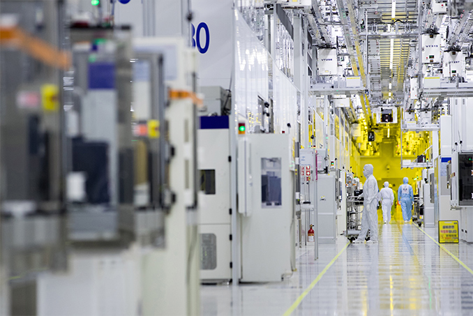
Samsung reportedly plans to invest billions of dollars to expand its 3D NAND production facility in Xian, China. If the company proceeds with the plan, bit production capacity of the fab would increase significantly.
According to Chinese media, the world’s largest supplier of NAND flash memory reportedly intends to spend $8 billion on expansion of its fab in Xian. Back in 2017, Samsung already announced plans to invest $7 billion over the following three years to boost the production capacity of its Xian facility, so the new investment will be spent on a third expansion of the fab.
Physical expansion of the Xian production facility will allow Samsung to further increase its 3D NAND bit output, giving Samsung more physical capacity and helping to offset the longer and more intensive manufacturing process required for high layer counts in 3D NAND. According to a media report, Samsung's Xian fab can now process 120,000 wafer starts per month. After the expansion, it will reportedly increase its output to 130,000 wafer starts per month, but it is likely that these will be 3D NAND wafers with a higher number of layers.
Samsung has not formally confirmed the $8 billion investment plan, but earlier this year the company indicated that it would be ‘flexible’ in expanding the Xian production facility.
Samsung currently produces 3D NAND at three sites: in Hwaseong and Pyeongtaek in South Korea and Xian in China.
Related Reading:
- NAND Flash Revenue Peaks in Q3 Amid Production Cuts & Outages
- Western Digital: Nearly All NAND Capacities Resumed Normal Operations
- SK Hynix NAND Update: 3D NAND Output Cut, Slowdown Capacity Expansions
- Toshiba & WD NAND Production Hit By Power Outage: 6 Exabytes Lost
- Micron: Shipments of 3D QLC for SSDs Nearly Double QoQ as Wafer Starts Cut Again
- Intel Memory Plans: No New NAND Capacity, Wants to Move 3D XPoint Production to China
- Boom to Bust: Memory Makers Plan to Cut NAND Flash Production
Sources: Reuters, Pulse News


5 Comments
View All Comments
coburn_c - Tuesday, December 17, 2019 - link
So the Chinese Media said Samsung was investing but Samsung itself didn't confirm it and you went ahead and published?coburn_c - Tuesday, December 17, 2019 - link
'reportedly' 'If' 'would' 'According to' 'reportedly' 'According to' 'will reportedly' 'not formally confirmed' '‘flexible’'These are all code words for this is not news.
s.yu - Wednesday, December 18, 2019 - link
Not Xian, Xi'an.edzieba - Wednesday, December 18, 2019 - link
Assuming the $8bn includes the previously confirmed $7bn, that's a $1bn fab investment for an 8% wafer start increase. Goes to show how much more complex modern processes are, and how that complexity is continuing to increase.soresu - Wednesday, December 18, 2019 - link
The latest process (136 layer, 6th gen) is actually less complex than the previous based on Anandtech's article on it.