Bridged or Native: Six of One, Half Dozen of Another?
Before looking at how NV45 solves some of NVIDIA's problems, we must first learn what those problems are. To understand this, we need to take a step back and look at the transition to PCI Express on a larger scale, and why ATI chose native while NVIDIA decided on bridged.If ATI had gone with a bridged solution rather than native, we wouldn't even be having this discussion. Their choice to go native was based on their internal assessment of the playing field. Obviously, we will eventually end up with all GPUs sporting native PCIe interfaces. Bridging does add a little latency and reduces the maximum possible bandwidth benefit from PCIe (especially if it wasn't possible to overclock the AGP interface to what would be 16x speeds as NVIDIA has done with their solution). Native solutions are also easier for OEM's to integrate onto their boards. Based on all this, we can't really say that ATI made a bad decision to go with native PCI Express. So, why did NVIDIA take a difference stance on the issue?
NVIDIA is trying to be cautious about the issue. With native PCI Express support, it would be necessary to fabricate twice as many different types of GPUs as it currently does with the only difference being the PCIe interface. Regardless of the size of a company, putting an ASIC to silicon is not something to be taken lightly (it's really expensive, especially when talking about potentially low yield (222M transistor) parts). At the same time, with separate GPUs specifically targeted at PCIe, it is necessary to estimate how many PCIe parts will be needed. This means estimating the adoption rate of PCIe. It's much easier to make a bunch of GPUs and bridges and play it by ear. This all makes logical sense, and as long as there is a negligible impact on performance and costs (in other words, value) delivered to the end users, we can't fault NVIDIA for going in this direction.
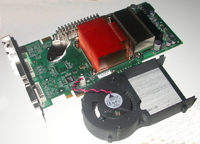
NV45 without the fan and shroud installed.
And since we've shown performance not to be an issue, in terms of the end users, only cost remains to be seen. Of course, in our assessment of why NVIDIA went with a bridge, we didn't answer one of the advantages that ATI has with its native solution: ease of integration by OEMs. More importantly, the disadvantage of the bridge solution isn't simply the inclusion of another discreet component (and another possible point of failure), but the continued need to route another parallel bus on an already packed card. Granted, the close proximity of the HSI to the GPU on NVIDIA cards makes the routing problem much less significant, but it would still be easier just to route serial lines from the connector to the GPU.
There are multiple squishy issues surrounding this, so we will do a little speculation using what we know as a basis. OEMs are essentially locked into selling their video cards at set price points, such as the current famous $499, $399, and $299 targets. They can't be competitive unless they meet these goals. They can't meet these goals and stay profitable unless ATI and NVIDIA keep the cost of their components down. It's certainly more cost effective for NVIDIA to pass on the cost of a bridge chip along with its GPUs than for ATI to have to deal with the impact of constructing a whole separate line of parts. Of course, we have no clue what kind of prices that ATI and NVIDIA charge for their components. As there is competition in the market place, it would make sense for parts targeted at similar markets to have similar prices. But how much does NVIDIA take into consideration the integration cost increase of its bridge to OEMs? Maybe, if ATI has to charge more to cover its fabrication costs and NVIDIA has some room to breathe, they can. But it's more likely that the OEMs would have to eat the cost, or pass it on to the consumer.
The unfortunate bottom line is that we really don't know the facts and details of what goes on behind the scenes, but there is a certain allure to not having to deal with a discrete bridge component. So, what's an IHV who's decided against native support to do? Enter NV45.


14 Comments
View All Comments
Pete - Thursday, July 1, 2004 - link
Thanks much for the prompt reply, Derek.DerekWilson - Wednesday, June 30, 2004 - link
PPro cahce was a seperate hunk of silicon nudged right up next to the core ;-) search google images for pentium pro and you'll see the what it looked like under there.Pete,
#1 not sure when that's going to happen, but it will be enevitable for both companies. How we get there is the question. ;-)
#2 our demo is the same, only drivers have changed from our previous tests. We are looking into IQ also...
hope that helps,
Derek Wilson
Pete - Tuesday, June 29, 2004 - link
Sorry, Derek, please ignore #3. For some reason I missed that you specified the 6800U (PCIe) was a custom-clocked NV45.Pete - Tuesday, June 29, 2004 - link
Hi Derek,Can you help clarify three things?
1. I remember reading that ATi would eventually move to all-PEG-native GPUs, and then use a bridge for AGP cards, similar to nV's future plans. Did you hear anything about this from ATi or their OEMs/partners?
2. Did you change your Far Cry demo, or are new drivers responsible for the impressive gains the 6800U has made to significantly overtake the X800XT(PE)?
3. The "NV45" in your charts is simply a higher-clocked "6800U (PCIe)," right? Did you down-clock the NV45 to attain the 6800U PCIe numbers used in Anand's earlier LGA article?
KF - Monday, June 28, 2004 - link
I'm not sure how garbled a recollecton can be, Minotaar. That's not the way I remember it. The PPro had the cache on separate chips in a complex package that plugged into a socket. PIIs, slot cartridge style, had separate cache chips at first, and no cache chips for the first Celeron, true. Later PIIs, and PII style Celerons had on-die full speed cache. On die, reduced size, cache for such as the notable 300 MHz (not 266) Celery that OCed 1.5x by setting the bus speed to 100 instead of 66.Back to the subject, There are some very odd results for a solution that is supposed to be, and mostly is, equal between AGP and PCIe.
GTMan32 - Monday, June 28, 2004 - link
There was a web site reporting that NVIDIA opened up one of ATIs PCIe chips and found it wasn't native but just had the bridging on-chip like the NV45.Then there was another comment that the ATI PCIe chips were clocked lower because of OEM fears that they were running too hot at the same speed as the AGP parts.
One could conclude that the tacked on AGP->PCIe bridge was causing this since it would be the same size as the AGP plus the extra circuits for the bridge. If the ATI solution was really native then it shouldn't have any heating problems?
But was all this just a rumor. I haven't heard anything on this since.
OCedHrt - Monday, June 28, 2004 - link
A possible explanation for the drop in performance on the PCIe cards could be due to specific optimizations that aren't enabled for the PCIe cards in the current drivers. Just a wild guess.ZobarStyl - Monday, June 28, 2004 - link
This bridging seems to be the perfect solution for first generation PCI-E chips which have nothing to gain over AGP anyway...just so long as nV doesn't get lazy and has a native PCI-E card by next gen (which might actually use the bandwidth), they really haven't lost anything with this solution. Good article.Filibuster - Monday, June 28, 2004 - link
Minotaar,The Pentium Pro, by todays standards, *does* have on package cache because it was not part of the cpu core. It is full cpu speed however.
http://members.iweb.net.au/~pstorr/pcbook/images/p...
The big deal about the Pentium 2 cache was that Intel had to make it that way so they could test the cache chips separately from the cpu and thus save money, because the PPRo was soo expensive.
Wonga - Monday, June 28, 2004 - link
-----Pentium Pro also had the advantage of clock speed cache, whereas P2's cache was bus speed.
-----
Well, if we want to be correct about everything, the P2's cache was not run at bus speed, but instead a fraction of the core speed. Half the core speed, to be precise.
Anyway, cheers for the review. Looks like nVidia listened to their OEM partners here and did the sensible thing bringing the HSI on package.