Intel Lists New Atom Core: Tremont to Come After Goldmont Plus
by Anton Shilov on April 23, 2018 5:00 PM EST
Intel has recently updated its developer documentation for instruction set extensions, and in the process has disclosed information on both new instructions for and the codename of its next-generation low-power processor microarchitecture. Dubbed "Tremont", the forthcoming processor core look to replace Goldmont Plus in the upcoming Atom, Celeron, and Pentium Silver-branded SoCs.
According to the Intel Architecture Instruction Set Extensions (ISE) and Future Features Programming Reference document, the Goldmont Plus microarchitecture will not be the end of the road for Intel’s low-cost/low-power cores. In the coming years it will be succeeded by the codenamed Tremont microarchitecture and its successors. On the manufacturing side of matters, nothing has officially been disclosed, but right now our suspicion is that processors based on the Tremont will be made using the company’s 10 nm process technology. To date we haven't seen Intel use their enhanced “+” and “++” 14nm process technologies to make SoCs for entry-level and energy-efficient PCs - as the original 14nm provides better density - so it seems unlikely that Intel would start now.
A key question about the Tremont is what architecturaly improvements it will bring. While Intel's document does specify the new instructions, it doesn't offer any general architectural insight. Intel's general trend thus far since Silvermont has been to gradually widen their out-of-order execution design, starting with two-way, moving to three-way (Goldmont), and then to a three-way front-end plus a four-way allocation and retirement backend. So it may be that we see Intel go this route, as they already have a number of tricks left in their bag from Core, and it meshes well with the high density aspects of their 10nm processes, which favors more complex processors.
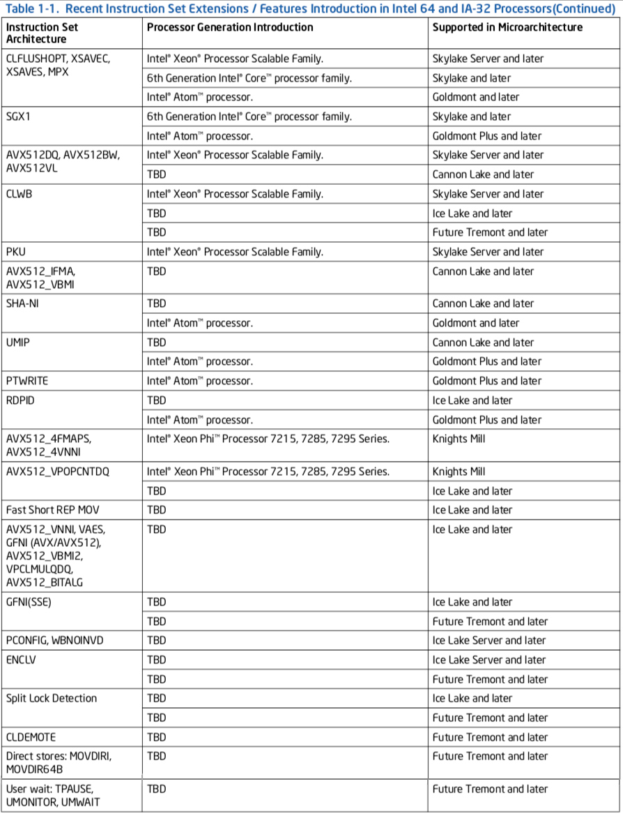
As for the ISE improvements, Intel’s Tremont will feature CLWB, GFNI (SSE-based), ENCLV, and Split Lock Detection instruction set extensions, which are also set to arrive with Intel’s Ice Lake processors. Also set to arrive with Tremont will be CLDEMOTE, direct store, and user wait instructions (see details in the table below). Unlike the earlier instructions, these are unique to Tremont and are not scheduled to be supported by the Ice Lake (or other documented Intel’s cores).
| New Instruction Set Extensions of Goldmont Plus and Tremont CPUs | |||||
| Instruction | Purpose | Description | |||
| Goldmont Plus | PTWRITE Write Data to a Processor Trace Packet |
Debugging | Unclear. | ||
| UMIP User-Mode Instruction Prevention |
Security | Prevents execution of certain instructions if the Current Privilege Level (CPL) is greater than 0. If these instructions were executed while in CPL > 0, user space applications could have access to system-wide settings such as the global and local descriptor tables, the task register and the interrupt descriptor table. | |||
| RDPID Read Processor ID |
General | Quickly reads processor ID to discover its feature set and apply optimizations/use specific code path if possible. | |||
| Tremont | CLWB Cache Line Write Back |
Performance | Writes back modified data of a cache line similar to CLFLUSHOPT, but avoids invalidating the line from the cache (and instead transitions the line to non-modified state). CLWB attempts to minimize the compulsory cache miss if the same data is accessed temporally after the line is flushed if the same data is accessed temporally after the line is flushed. | ||
| GFNI (SSE) | Security | SSE-based acceleration of Galois Field Affine Transformation alghorithms. | |||
| ENCLV | Security | Further enhancement of SGX version 1 capabilities. | |||
| CLDEMOTE | Performance | Enables CPU to demote a cache line with a specific adress from the nearest cache to a more distant cache without writing back to memory. Speeds up access to this line by other cores within a CPU. | |||
| Direct stores: MOVDIRI, MOVDIR64B | Performance | ||||
| User wait: TPAUSE, UMONITOR, UMWAIT | Power | Direct CPU to enter certain stages before an event happens. | |||
| Split Lock Detection | |||||
| Source: Intel Architecture Instruction Set Extensions and Future Features Programming Reference (pages 12 and 13) | |||||
The fact that Intel is readying its “Future Tremont and later” microarchitectures reveals that even after the company withdrew from smartphone SoCs, it sees plenty of applications that could use its low-power/low-cost Atom cores. There is sitll a notable market for budget PCs as well as embedded and semi-embeded markets for items like IoT edge devices, all of which Intel intends to continue serving with the line of smaller, cheaper cores. Meanwhile, consistent ILP and performance improvements as well as introduction of new ISEs to these microarchitectures show that Intel wants these cores to offer competitive performance to other low-cost processors, while still maintaining near feature set parity to Intel's high-performance cores.
Related Reading
- Intel Launches New Pentium Silver and Celeron Atom Processors: Gemini Lake is Here
- Intel Documents Point to AVX-512 Support for Cannon Lake Consumer CPUs
- Intel Quietly Launches Apollo Lake SoC: Goldmont CPU, 6 SKUs, 6 & 10 Watts
- Intel's Changing Future: Smartphone SoCs Broxton & SoFIA Officially Cancelled


56 Comments
View All Comments
mode_13h - Monday, April 23, 2018 - link
Cue the Atom haters and countless Atom vs. ARM specs wars and benchmark battles...HStewart - Monday, April 23, 2018 - link
I think most people truly don't understand what Atom is used for - in my opinion I believe one of purpose is for Intel to use as test bed for SOC in moving the whole system on single chip.Technologies like Phi ( using many cores ) and Y and even U series come from this research.
I have one the newer Pentium based machines - it is significantly slower than other machines today - but similar speed to older machines like Core 2 and possibly my Surface Pro.
Speed is relevant to time it made - even the slowest atom will be faster that fastest machines 15 or 20 years ago.
It been a long time, like almost 25 years - but I used to do serious stuff with these Intel manuals - when they were actually physical pieces of paper. At first when I read this chart - I thought the Atom had AVX512 - I would like to see even the strongest ARM compete with that.
mode_13h - Monday, April 23, 2018 - link
I miss the days when you could just call or email Intel and they'd send you a free set of bound, printed manuals. I still have my last set.HStewart - Monday, April 23, 2018 - link
During my OS days, I remember going over to local Intel office in Atlanta with co-working and picking up Intel manuals for free because of my job - my favorite was the 386 Operating System writers guide - the last manual I got has paper was the sort of tan-gray Pentium manual - I had to purchase that one. I just pull out the original purple and black i486 manual next to Transputer manual from my book shelf in my bedroom. It is in pretty rough shape from my 1st job of seven years. We did get AMD manuals - not sure if they even have the specs on those now a days - back then the AMD chips were basically a clone of Intel chips - I not sure even CPUID could detect difference.mode_13h - Monday, April 23, 2018 - link
I remember reading about Transputers. Fun to think about, back then. Years later, I had a professional encounter with (one of?) its descendent(s).mode_13h - Tuesday, April 24, 2018 - link
It's interesting to see that mesh architectures and many of the purported applications of Transputers (AI, etc.) have now become mainstream.close - Tuesday, April 24, 2018 - link
Phi has nothing to do with Atom. It was based on the GPU research that Intel did. Neither core design, nor manufacturing really relied on the research put into Atom.And the fact that Atom is faster than a 20 years old CPU is pretty much irrelevant.
But what is relevant is the comparison to ARM. Since they both target the same low TDP space, the same usage scenarios, and more or less the same user base why wouldn't it be? There's a reason Atom based mobile devices never took off. They're either too slow in the low TDP, or have too high TDP in the higher performance models. And that's after Intel went through years of iterating and improving. If you look at what Apple managed to achieve with their A SoCs in just a few generations you start to see the limits and potential of each architecture or instruction set.
Drumsticks - Tuesday, April 24, 2018 - link
That first half is definitely not true. Phi is/was a combination of both. It was certainly originally based on the GPU research intel did, but the x86 core within the Knight's Landing line was unmistakably built off of Silvermont.mode_13h - Tuesday, April 24, 2018 - link
You're both right.The original Larrabee had Pentium P54C-derived cores, which were carried through to the first Xeon Phi (Knights Corner). The second generation of Xeon Phi uses Silvermont Atom-derived cores. I don't know if they've said what Knights Mill uses, but it's sort of a half-generation, with some some hastily-added deep learning optimizations.
And before all of that (back in 2007) came Intel's 80-core TFLOPS research chip, which I this was reported to utilize some sort of RISC cores.
close - Wednesday, April 25, 2018 - link
It started off from old Pentium cores and it started as GPU research. They gave up on the GPU dream because it was obviously not suited for that and decided to target the accelerator market.Then they replaced the cores they were using with Atom cores but not because the Atom was a diamond in the mud. They did it because... "it was laying around" so to speak. :) Intel didn't have any other core that they could cram more than a handful of in one package and developing a whole new one made no sense. So they took the core they already had and that fit the bill: relatively low power, somewhat performant. But Phi itself wasn't designed with Atom in mind.
The Atom isn't a benchmark in any respect, unfortunately. It was the last pick on the dodge team when it came to Phi. And it's usually the last pick for anything since there are better options, ones with less compromises.