The Crucial MX500 500GB SSD Review: A Second Look
by Billy Tallis on February 2, 2018 9:30 AM ESTConclusion
This second look at the Crucial MX500 reinforces our opinion of it as a solid performer, but it definitely isn't the fastest TLC SSD around. It is more common to find the MX500 placing second or third in its class on the performance tests, which isn't a problem if the price is right.
The 500GB MX500 is clearly slower than the 1TB model, and at first glance its performance relative to the competition is not as impressive as the results from the 1TB model. The 500GB capacity class is starting to become the default choice over smaller sizes, but it is no longer big enough to offer full performance even on drives that are limited by the SATA interface. On the other hand, the per-die capacity of the MX500's 64-layer 3D TLC is actually lower than that of the 32L 3D TLC used by the MX300, so the 250GB model shouldn't be as handicapped as the smallest MX300 was.
Since our first look at the Crucial MX500, the Samsung 860 PRO has raised the bar again for SATA SSDs. However, it exists in a price bracket that has been taken over by NVMe SSDs, so it isn't really serious competition for mainstream SATA drives. It is the TLC-based 860 EVO that will really matter. Samsung has clearly refined both their controller and their NAND, and we expect the 860 EVO to improve over the 850 EVO in both performance and power consumption.
When the dust settles on this round of product launches, Crucial will probably once again be in the position of offering a slower but cheaper option than Samsung's mainstream SATA drive. But this time around, the performance gap will be much smaller, and the MX500 comes with far fewer caveats than the MX300. The MX500 doesn't have serious performance problems when full like the MX300 and many other entry-level SSDs. The warranty and write endurance ratings are decent, and the MX series still matches Samsung's SSDs for features like drive encryption.
| SATA SSD Price Comparison | ||||
| 240-275GB | 480-525GB | 960-1050GB | 2TB | |
| Crucial MX500 | $79.99 (32¢/GB) | $134.95 (27¢/GB) | $259.99 (26¢/GB) | $499.99 (25¢/GB) |
| Crucial BX300 | $87.99 (37¢/GB) | $144.99 (30¢/GB) | ||
| Crucial MX300 | $92.99 (34¢/GB) | $147.45 (28¢/GB) | $274.99 (26¢/GB) | $546.23 (27¢/GB) |
| Samsung 850 EVO | $99.99 (40¢/GB) | $149.99 (30¢/GB) | $299.99 (30¢/GB) | $696.00 (35¢/GB) |
| Samsung 860 EVO | $94.99 (38¢/GB) | $169.99 (34¢/GB) | $329.99 (33¢/GB) | $649.99 (32¢/GB) |
| SanDisk Ultra 3D | $79.99 (32¢/GB) | $139.99 (28¢/GB) | $249.99 (25¢/GB) | $549.99 (27¢/GB) |
| WD Blue 3D NAND | $79.99 (32¢/GB) | $139.96 (28¢/GB) | $259.99 (26¢/GB) | $529.99 (26¢/GB) |
| Samsung 850 PRO | $155.00 (61¢/GB) | $219.99 (43¢/GB) | $429.99 (42¢/GB) | $888.61 (43¢/GB) |
| Samsung 860 PRO | $139.99 (55¢/GB) | $249.99 (49¢/GB) | $479.99 (47¢/GB) | $949.99 (46¢/GB) |
| ADATA SU800 | $78.50 (31¢/GB) | $139.99 (27¢/GB) | ||
| Toshiba TR200 | $79.99 (33¢/GB) | |||
| Intel 545s | $89.99 (35¢/GB) | $149.99 (29¢/GB) | ||
Crucial and Samsung are both making quick transitions to their new models: the MX300 and the 850 series SSDs are starting to go out of stock and their prices are climbing. The full range of MX500 capacities are now mostly in stock, as are most of the Samsung 860 PROs and EVOs, and they're all still pretty much stuck at MSRP. Even at MSRP, the Crucial MX500 is priced to beat all the other SATA SSDs using 64L 3D NAND, and it more or less matches the older and slower models that are still available.
Other SSD manufacturers don't seem to have fully reacted yet to the Crucial MX500's pricing. The Western Digital WD Blue 3D/SanDisk Ultra 3D is almost as fast as the MX500 and almost as cheap, so it's a good product to keep an eye on, but not the one to buy if you're buying today (except at 1TB, where the Ultra 3D is $10 cheaper).
The Intel 545s uses similar NAND and controller to the MX500 but usually comes out slightly ahead. However, Intel hasn't been pricing the 545s very aggressively and they haven't released 1TB or 2TB capacities. Toshiba's DRAMless TR200 is barely a presence on the market with only the 240GB model in stock and at a price no cheaper than mainstream drives. The many other brands that don't manufacture their own NAND flash are using the 64L 3D NAND they can acquire for PCIe SSDs, so the rest of the competition for the MX500 is last-generation SATA drives.

The MX500 is one of the cheapest SSDs on the market at the moment, and it offers real-world performance very close to the Samsung 850 EVO. This makes it very easy to recommend.
The only caveat to that recommendation is that power efficiency has taken a step backwards with the MX500, while Samsung appears to be setting new records in that department with the 860 series. We expect our upcoming testing of the 860 EVO to show it using less power than the MX500 and probably offering slightly better performance. But at the moment it looks like those probable advantages come at a pretty steep premium.


25 Comments
View All Comments
PeachNCream - Friday, February 2, 2018 - link
"..the per-die capacity of the MX500's 64-layer 3D TLC is actually lower than that of the 32L 3D TLC.."Why is that the case? Shouldn't doubling the number of layers lead to greater capacity and does this mean that there are more ICs per GB in the newer MX500? I'm super confused.
jtd871 - Friday, February 2, 2018 - link
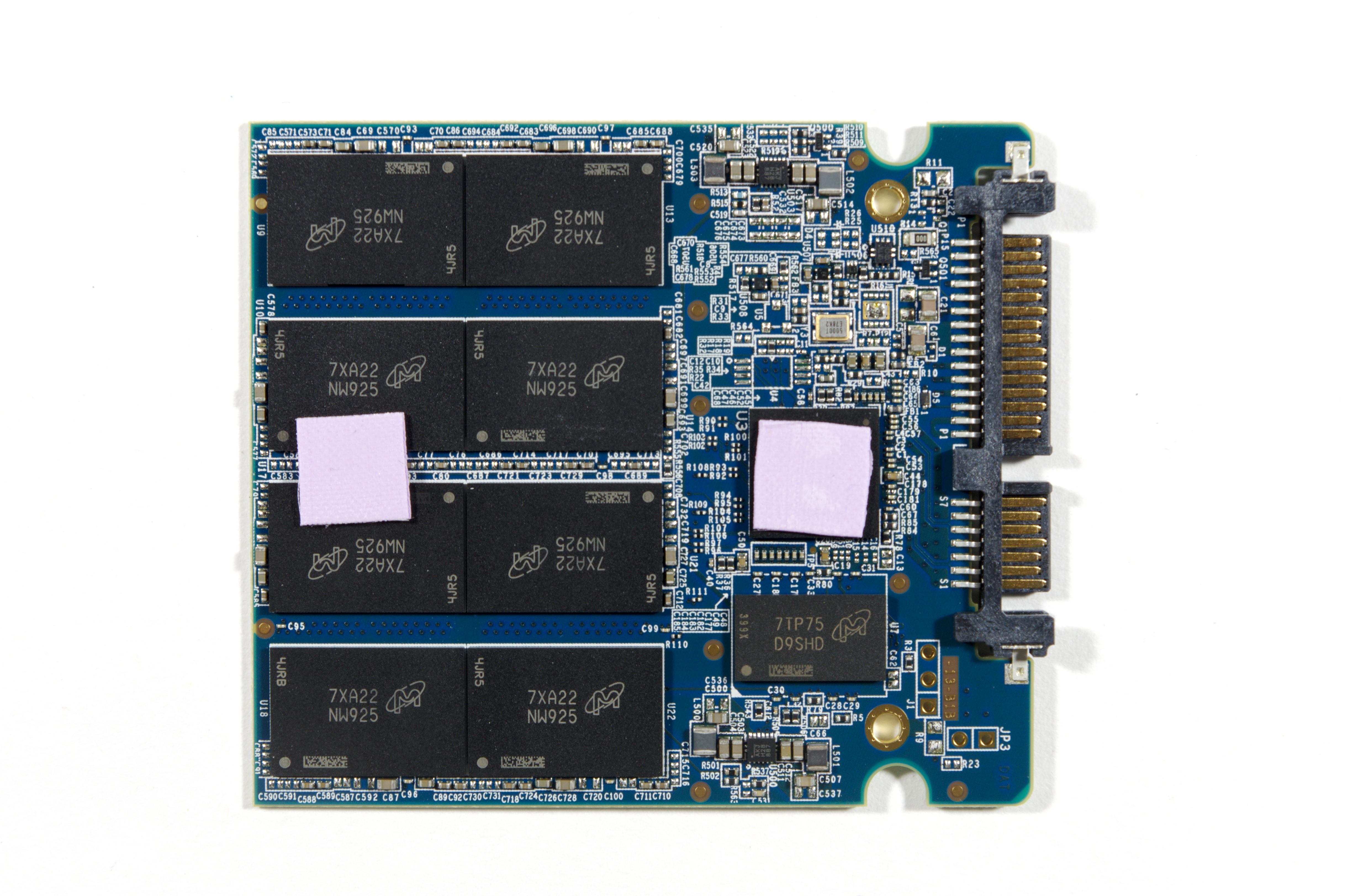
"The Crucial MX500 uses Micron's 256Gb 64L 3D TLC part and consequently returns to the standard drive capacities and overprovisioning ratios, instead of the unusual configurations caused by the 384Gb die capacity in the MX300's 32L 3D TLC. The slightly lower usable capacities of the MX500 than the MX300 means the new drives have slightly higher prices on a per-GB basis, but the MSRPs are still very competitive against current street prices for the competition."So the new chips have more layers per package, but less overall capacity. I'll guess the 384Gb die hamstrung performance on relatively smaller-capacity drives by offering fewer memory channels for the processor to work with simultaneously. Plus, I'll guess that it was a bit of an oddball size for the algorithms to deal with.
FunBunny2 - Friday, February 2, 2018 - link
large node?more area dedicated to control functions?
Billy Tallis - Friday, February 2, 2018 - link
For the 32L node, IMFT was more or less prioritizing MLC use cases by making a 256Gb MLC die that could be used as a 384Gb TLC part. For the 64L node, TLC is the priority and they're making both 256Gb TLC and 512Gb TLC parts. The latter should be cheaper per GB when it is available, but would be a worse choice for small consumer drives. The 256Gb die is really tiny, which makes it more appealing to the mobile market than a lot of previous IMFT parts.FunBunny2 - Saturday, February 3, 2018 - link
"making a 256Gb MLC die that could be used as a 384Gb TLC part."so... does this mean that NAND is all the same, and it's the controller that decides among S/M/T?? or is it the case that S can be coerced to M, and M to T, but not the other way round? is there a tute, here or elsewhere, that tells us the nittygritty about why titular NAND can/can't be used at other densities?
FunBunny2 - Saturday, February 3, 2018 - link
well, I did find one, but from 2012 (and AT: https://www.anandtech.com/show/5067/understanding-... )"This array can be turned into either SLC, MLC, or TLC. The actual array and transistors are equivalent in all three flash types; there is no physical difference. "
some/many folks have been claiming that TLC, in particular, is physically different from SLC. is that now true?
Kristian Vättö - Sunday, February 4, 2018 - link
In terms of memory cell design, SLC, MLC and TLC can be the same, but the peripheral circuit design isn't (min # of latches = # of bits per cell). More bits per cell designs are also likely to have more spare/ECC bytes per page.In layman terms, TLC and MLC can be run as pseudo-SLC by only programming the lower page, but it's impossible to run e.g. MLC as TLC. But pseudo-SLC isn't the same thing as native SLC.
Spatty - Wednesday, February 14, 2018 - link
SLC/MLC chips are physically the same chips during the fab process. Maybe some Implant changes but die layout is the same. In Probe, circuits are blown to make them SLC or MLC.The referenced quote in this thread, is that a due to the usage of die vs chip/package. The chips in the images can have multiple die in one single chip/package and thus the 'density' of the chip/package changes. More layers still means more bits/mm^2.
PeachNCream - Monday, February 5, 2018 - link
Thanks Billy! It makes more sense now.colonelclaw - Friday, February 2, 2018 - link
I'm wondering, would it be worth adding a PS4 Pro/'BoneX benchmark to SATA SSD reviews? The 1TB is fast becoming a worthwhile, if luxurious, upgrade for the top consoles. It may be slightly unaffordable now, but possibly not for long?