The Crucial MX500 500GB SSD Review: A Second Look
by Billy Tallis on February 2, 2018 9:30 AM ESTMixed Random Performance
Our test of mixed random reads and writes covers mixes varying from pure reads to pure writes at 10% increments. Each mix is tested for up to 1 minute or 32GB of data transferred. The test is conducted with a queue depth of 4, and is limited to a 64GB span of the drive. In between each mix, the drive is given idle time of up to one minute so that the overall duty cycle is 50%.
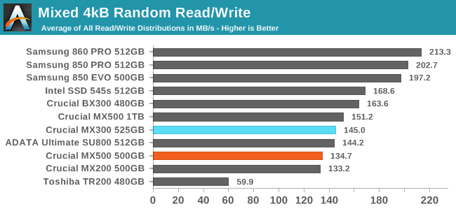
The mixed random I/O performance of the Crucial MX500 is slower overall than the MX300 and most of the current-generation competition. Even the faster 1TB model is a bit below average among half-TB drives.
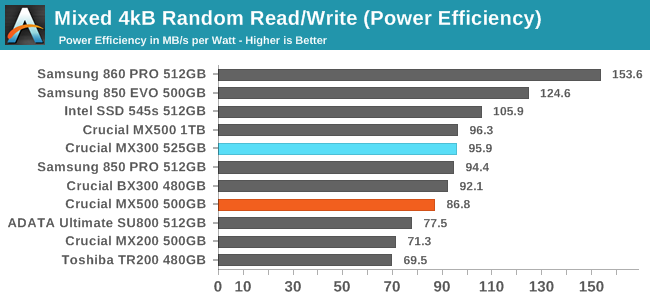
The power efficiency of the MX500 on the mixed random I/O test has also regressed a bit, but it isn't much below par—only Samsung's drives really stand out as quite efficient on this test.
 |
|||||||||
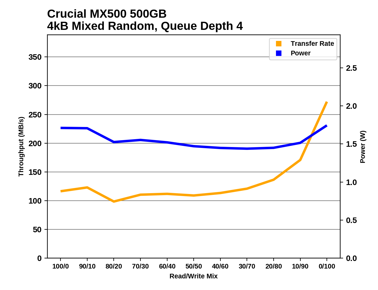
The Crucial MX500's performance is a bit unsteady during the first half of this test, before climbing through the second half as the opportunities for combining and caching writes increase. Most of the competition shows much steadier performance increases across the entire test, though not always with such a pronounced spike at the end.
Mixed Sequential Performance
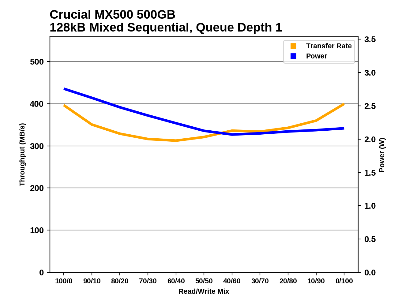
Our test of mixed sequential reads and writes differs from the mixed random I/O test by performing 128kB sequential accesses rather than 4kB accesses at random locations, and the sequential test is conducted at queue depth 1. The range of mixes tested is the same, and the timing and limits on data transfers are also the same as above.
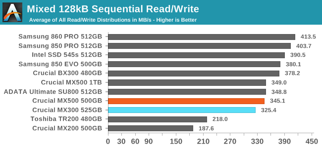
The mixed sequential I/O performance of the MX500 is a slight improvement over the MX300, but it is still a bit slower than the 850 EVO or Intel 545s, and the MLC drives have a clear advantage.
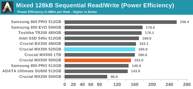
While performance improved slightly, the Crucial MX500's power efficiency on the mixed sequential I/O test was a bit worse than the MX300. Aside from the big efficiency jump from the Samsung 860 PRO, the differences between the MX500 and the competition are small, but there's room for improvement.
 |
|||||||||
The performance curves for the two capacities of the Crucial MX500 show the same basic shape, with the drives performing the worst on mixes of about 60% reads. Samsung's drives bottom out in the second half of the test with mixes of around 30% reads, and the Intel 545s doesn't have any clear weak spot but its performance wavers slightly throughout the mixed sequential I/O test.


25 Comments
View All Comments
PeachNCream - Friday, February 2, 2018 - link
"..the per-die capacity of the MX500's 64-layer 3D TLC is actually lower than that of the 32L 3D TLC.."Why is that the case? Shouldn't doubling the number of layers lead to greater capacity and does this mean that there are more ICs per GB in the newer MX500? I'm super confused.
jtd871 - Friday, February 2, 2018 - link
"The Crucial MX500 uses Micron's 256Gb 64L 3D TLC part and consequently returns to the standard drive capacities and overprovisioning ratios, instead of the unusual configurations caused by the 384Gb die capacity in the MX300's 32L 3D TLC. The slightly lower usable capacities of the MX500 than the MX300 means the new drives have slightly higher prices on a per-GB basis, but the MSRPs are still very competitive against current street prices for the competition."So the new chips have more layers per package, but less overall capacity. I'll guess the 384Gb die hamstrung performance on relatively smaller-capacity drives by offering fewer memory channels for the processor to work with simultaneously. Plus, I'll guess that it was a bit of an oddball size for the algorithms to deal with.
FunBunny2 - Friday, February 2, 2018 - link
large node?more area dedicated to control functions?
Billy Tallis - Friday, February 2, 2018 - link
For the 32L node, IMFT was more or less prioritizing MLC use cases by making a 256Gb MLC die that could be used as a 384Gb TLC part. For the 64L node, TLC is the priority and they're making both 256Gb TLC and 512Gb TLC parts. The latter should be cheaper per GB when it is available, but would be a worse choice for small consumer drives. The 256Gb die is really tiny, which makes it more appealing to the mobile market than a lot of previous IMFT parts.FunBunny2 - Saturday, February 3, 2018 - link
"making a 256Gb MLC die that could be used as a 384Gb TLC part."so... does this mean that NAND is all the same, and it's the controller that decides among S/M/T?? or is it the case that S can be coerced to M, and M to T, but not the other way round? is there a tute, here or elsewhere, that tells us the nittygritty about why titular NAND can/can't be used at other densities?
FunBunny2 - Saturday, February 3, 2018 - link
well, I did find one, but from 2012 (and AT: https://www.anandtech.com/show/5067/understanding-... )"This array can be turned into either SLC, MLC, or TLC. The actual array and transistors are equivalent in all three flash types; there is no physical difference. "
some/many folks have been claiming that TLC, in particular, is physically different from SLC. is that now true?
Kristian Vättö - Sunday, February 4, 2018 - link
In terms of memory cell design, SLC, MLC and TLC can be the same, but the peripheral circuit design isn't (min # of latches = # of bits per cell). More bits per cell designs are also likely to have more spare/ECC bytes per page.In layman terms, TLC and MLC can be run as pseudo-SLC by only programming the lower page, but it's impossible to run e.g. MLC as TLC. But pseudo-SLC isn't the same thing as native SLC.
Spatty - Wednesday, February 14, 2018 - link
SLC/MLC chips are physically the same chips during the fab process. Maybe some Implant changes but die layout is the same. In Probe, circuits are blown to make them SLC or MLC.The referenced quote in this thread, is that a due to the usage of die vs chip/package. The chips in the images can have multiple die in one single chip/package and thus the 'density' of the chip/package changes. More layers still means more bits/mm^2.
PeachNCream - Monday, February 5, 2018 - link
Thanks Billy! It makes more sense now.colonelclaw - Friday, February 2, 2018 - link
I'm wondering, would it be worth adding a PS4 Pro/'BoneX benchmark to SATA SSD reviews? The 1TB is fast becoming a worthwhile, if luxurious, upgrade for the top consoles. It may be slightly unaffordable now, but possibly not for long?