The Crucial MX500 500GB SSD Review: A Second Look
by Billy Tallis on February 2, 2018 9:30 AM ESTSequential Read Performance
Our first test of sequential read performance uses short bursts of 128MB, issued as 128kB operations with no queuing. The test averages performance across eight bursts for a total of 1GB of data transferred from a drive containing 16GB of data. Between each burst the drive is given enough idle time to keep the overall duty cycle at 20%.
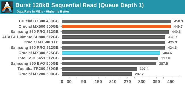
The Crucial MX500 is tied with the BX300 for fastest burst sequential read performance from SATA SSDs in this capacity range, even managing to beat the Samsung 860 PRO by a few MB/s.
Our test of sustained sequential reads uses queue depths from 1 to 32, with the performance and power scores computed as the average of QD1, QD2 and QD4. Each queue depth is tested for up to one minute or 32GB transferred, from a drive containing 64GB of data.
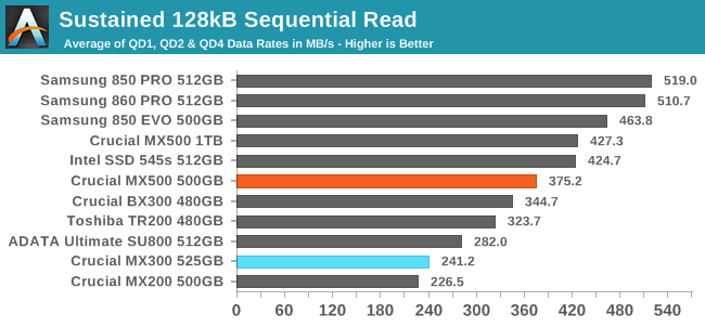
The sustained sequential read performance of the MX500 is much better than the MX300, but still not up to Samsung's level, and the 500GB MX500 is significantly slower than the 1TB model on this test.
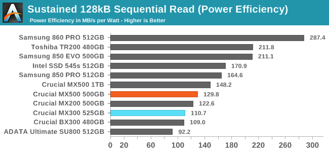
Crucial's power efficiency on the sustained sequential read test is still poor, and the 500GB MX500 is worse off than the 1TB model. Meanwhile, Samsung has significantly raised the bar with the 860 PRO.
 |
|||||||||
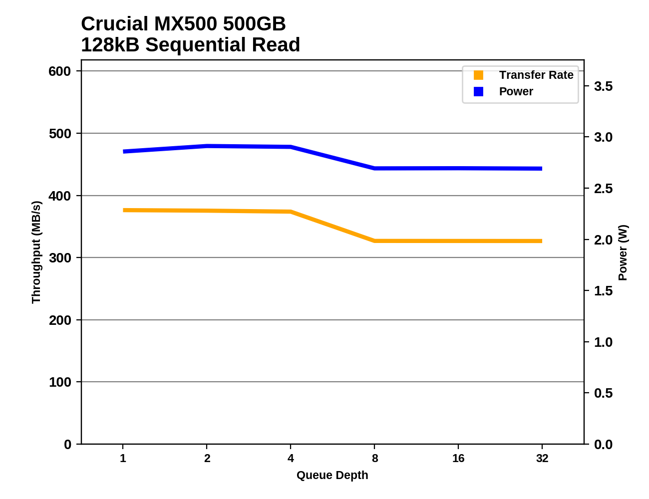
Unlike the 1TB MX500, the 500GB MX500 hits its full sequential read performance at QD1, but neither can maintain it through the entire test. The 1TB and 500GB models use almost exactly the same amount of power, but the 1TB model is significantly faster.
Sequential Write Performance
Our test of sequential write burst performance is structured identically to the sequential read burst performance test save for the direction of the data transfer. Each burst writes 128MB as 128kB operations issued at QD1, for a total of 1GB of data written to a drive containing 16GB of data.
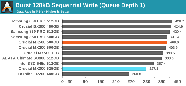
The burst sequential write performance of the Crucial MX500 is tied with the Samsung 850 EVO for being the fastest result from a TLC SSD. The 500GB MX500 scores slightly higher than the 1TB model, and is a big improvement over the MX300.
Our test of sustained sequential writes is structured identically to our sustained sequential read test, save for the direction of the data transfers. Queue depths range from 1 to 32 and each queue depth is tested for up to one minute or 32GB, followed by up to one minute of idle time for the drive to cool off and perform garbage collection. The test is confined to a 64GB span of the drive.
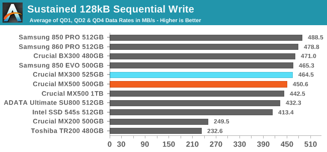
On the sustained sequential write test, the MX500 actually performs slightly worse than the MX300, but again the 500GB MX500 is a bit faster than the 1TB model. What was a tie between the MX300 and the 850 EVO last year is probably going to be a small but clear win this year for the 860 EVO over the MX500, but against other TLC drive the MX500 still looks great.
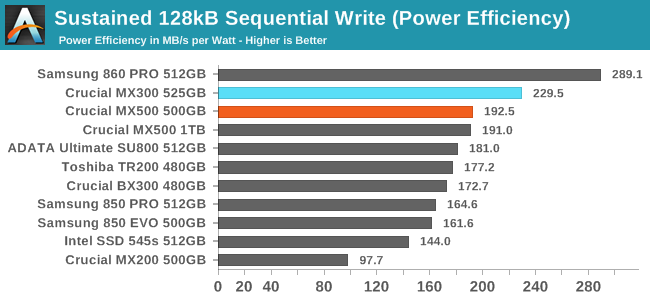
The two capacities of the Crucial MX500 show the same power efficiency during the sequential write test. They're less efficient than the MX300 was, but still near the top of the chart.
 |
|||||||||
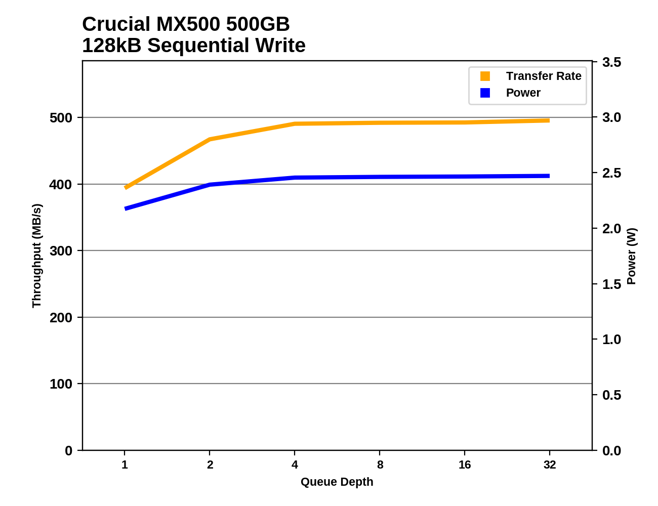
By QD4 the 500GB Crucial MX500 is almost at its full sequential write speed, and its performance steadily gains the last few percent over the rest of the test. At lower queue depths, the MX500 is actually slightly slower than the MX300, but the MX300 couldn't retain its performance for the entire test.


25 Comments
View All Comments
PeachNCream - Friday, February 2, 2018 - link
"..the per-die capacity of the MX500's 64-layer 3D TLC is actually lower than that of the 32L 3D TLC.."Why is that the case? Shouldn't doubling the number of layers lead to greater capacity and does this mean that there are more ICs per GB in the newer MX500? I'm super confused.
jtd871 - Friday, February 2, 2018 - link
"The Crucial MX500 uses Micron's 256Gb 64L 3D TLC part and consequently returns to the standard drive capacities and overprovisioning ratios, instead of the unusual configurations caused by the 384Gb die capacity in the MX300's 32L 3D TLC. The slightly lower usable capacities of the MX500 than the MX300 means the new drives have slightly higher prices on a per-GB basis, but the MSRPs are still very competitive against current street prices for the competition."So the new chips have more layers per package, but less overall capacity. I'll guess the 384Gb die hamstrung performance on relatively smaller-capacity drives by offering fewer memory channels for the processor to work with simultaneously. Plus, I'll guess that it was a bit of an oddball size for the algorithms to deal with.
FunBunny2 - Friday, February 2, 2018 - link
large node?more area dedicated to control functions?
Billy Tallis - Friday, February 2, 2018 - link
For the 32L node, IMFT was more or less prioritizing MLC use cases by making a 256Gb MLC die that could be used as a 384Gb TLC part. For the 64L node, TLC is the priority and they're making both 256Gb TLC and 512Gb TLC parts. The latter should be cheaper per GB when it is available, but would be a worse choice for small consumer drives. The 256Gb die is really tiny, which makes it more appealing to the mobile market than a lot of previous IMFT parts.FunBunny2 - Saturday, February 3, 2018 - link
"making a 256Gb MLC die that could be used as a 384Gb TLC part."so... does this mean that NAND is all the same, and it's the controller that decides among S/M/T?? or is it the case that S can be coerced to M, and M to T, but not the other way round? is there a tute, here or elsewhere, that tells us the nittygritty about why titular NAND can/can't be used at other densities?
FunBunny2 - Saturday, February 3, 2018 - link
well, I did find one, but from 2012 (and AT: https://www.anandtech.com/show/5067/understanding-... )"This array can be turned into either SLC, MLC, or TLC. The actual array and transistors are equivalent in all three flash types; there is no physical difference. "
some/many folks have been claiming that TLC, in particular, is physically different from SLC. is that now true?
Kristian Vättö - Sunday, February 4, 2018 - link
In terms of memory cell design, SLC, MLC and TLC can be the same, but the peripheral circuit design isn't (min # of latches = # of bits per cell). More bits per cell designs are also likely to have more spare/ECC bytes per page.In layman terms, TLC and MLC can be run as pseudo-SLC by only programming the lower page, but it's impossible to run e.g. MLC as TLC. But pseudo-SLC isn't the same thing as native SLC.
Spatty - Wednesday, February 14, 2018 - link
SLC/MLC chips are physically the same chips during the fab process. Maybe some Implant changes but die layout is the same. In Probe, circuits are blown to make them SLC or MLC.The referenced quote in this thread, is that a due to the usage of die vs chip/package. The chips in the images can have multiple die in one single chip/package and thus the 'density' of the chip/package changes. More layers still means more bits/mm^2.
PeachNCream - Monday, February 5, 2018 - link
Thanks Billy! It makes more sense now.colonelclaw - Friday, February 2, 2018 - link
I'm wondering, would it be worth adding a PS4 Pro/'BoneX benchmark to SATA SSD reviews? The 1TB is fast becoming a worthwhile, if luxurious, upgrade for the top consoles. It may be slightly unaffordable now, but possibly not for long?