The Crucial MX500 500GB SSD Review: A Second Look
by Billy Tallis on February 2, 2018 9:30 AM ESTRandom Read Performance
Our first test of random read performance uses very short bursts of operations issued one at a time with no queuing. The drives are given enough idle time between bursts to yield an overall duty cycle of 20%, so thermal throttling is impossible. Each burst consists of a total of 32MB of 4kB random reads, from a 16GB span of the disk. The total data read is 1GB.
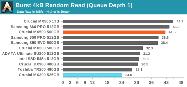
The 500GB Crucial MX500 isn't quite as fast as its 1TB sibling on the burst random read performance test, but it still scores better than any other TLC we've tested. The Samsung 860 EVO might be able to beat the MX500's performance here when it arrives, but probably not my much.
Our sustained random read performance is similar to the random read test from our 2015 test suite: queue depths from 1 to 32 are tested, and the average performance and power efficiency across QD1, QD2 and QD4 are reported as the primary scores. Each queue depth is tested for one minute or 32GB of data transferred, whichever is shorter. After each queue depth is tested, the drive is given up to one minute to cool off so that the higher queue depths are unlikely to be affected by accumulated heat build-up. The individual read operations are again 4kB, and cover a 64GB span of the drive.
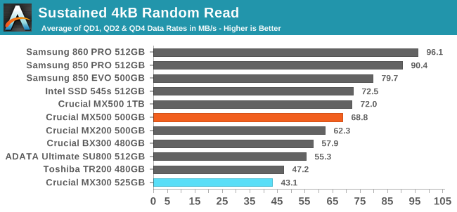
With longer queue depths and test run times, the MX500's random read performance falls from first place to merely above average. The MX500 is still the fastest Crucial SSD, but it is substantially slower than the Samsung SATA drives and is not quite as fast as the Intel 545s.
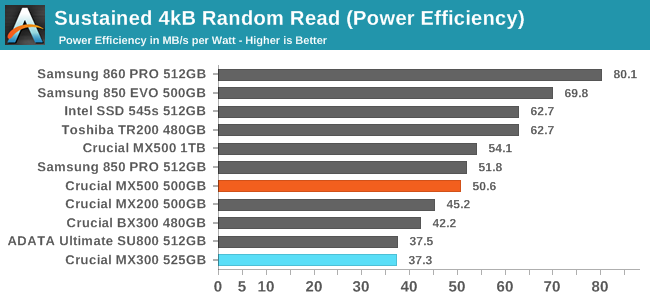
The power efficiency of the Crucial MX500 during the random read test is better than any previous Crucial SSD, but the Intel 545s and Samsung 850 EVO outscore it significantly. The 860 EVO will only widen this gap.
 |
|||||||||
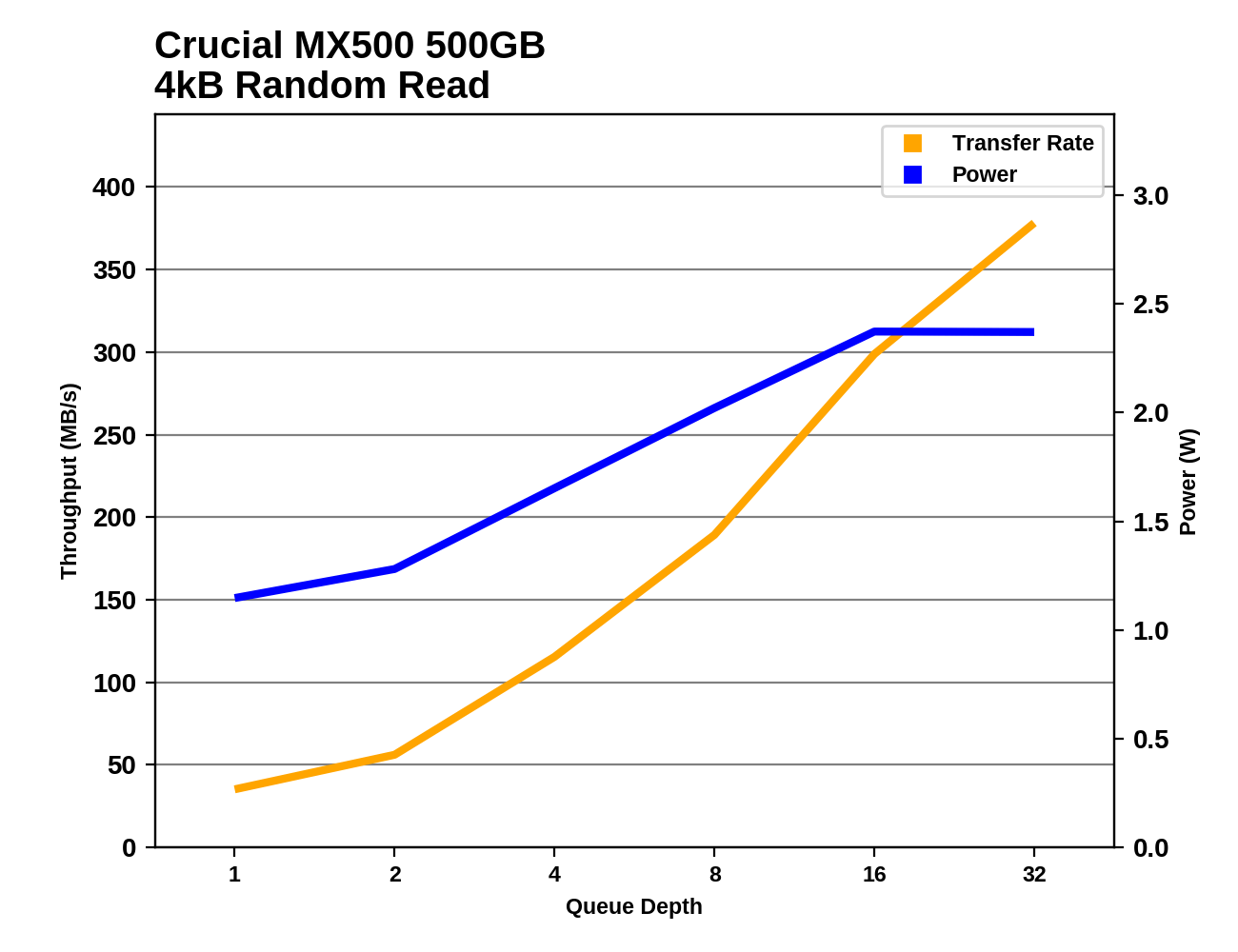
The Intel 545s and the Crucial MX500 perform about the same until QD16 where the 545s starts to level off. The Samsung 850 EVO starts building a lead on the MX500 at much lower queue depths, so it reach es peak performance much earlier. Both of those competitors use less power than the MX500 throughout the random read test.
Random Write Performance
Our test of random write burst performance is structured similarly to the random read burst test, but each burst is only 4MB and the total test length is 128MB. The 4kB random write operations are distributed over a 16GB span of the drive, and the operations are issued one at a time with no queuing.
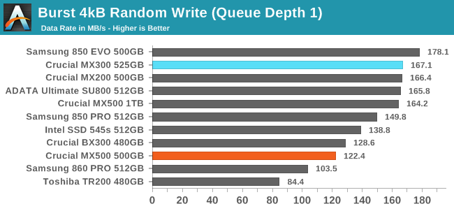
The burst random write speed of the 500GB Crucial MX500 is a disappointment, coming in slower than most of its competition and 25% slower than the 1TB model.
As with the sustained random read test, our sustained 4kB random write test runs for up to one minute or 32GB per queue depth, covering a 64GB span of the drive and giving the drive up to 1 minute of idle time between queue depths to allow for write caches to be flushed and for the drive to cool down.
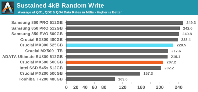
The Crucial MX500 500GB doesn't fare quite as badly on the longer random write test. It's still one of the slower drives in the bunch, but not by such a wide margin, and it is only a little bit slower than the 1TB model.
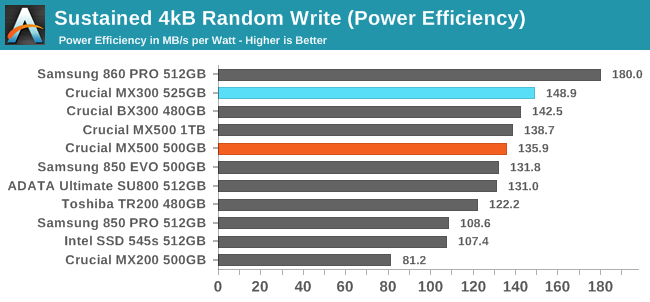
The Crucial MX500 has good power efficiency during random writes, but both the MX300 and BX300 are slightly better, and the Samsung 860 PRO's large lead suggests the 860 EVO may also be in competition for the most efficient TLC SSD.
 |
|||||||||
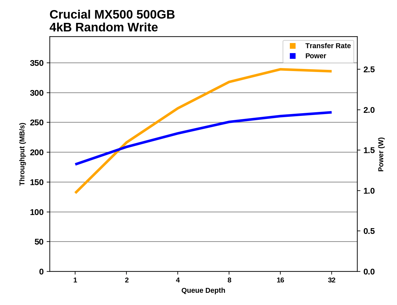
The Crucial MX500 takes longer to get up to speed than the Samsung 850 EVO, but it does eventually get up to full speed matching the best SATA SSDs. Previous Crucial SSDs and the Intel 545s struggle to get up to the level of Samsung's random write performance even at QD32.


25 Comments
View All Comments
PeachNCream - Friday, February 2, 2018 - link
"..the per-die capacity of the MX500's 64-layer 3D TLC is actually lower than that of the 32L 3D TLC.."Why is that the case? Shouldn't doubling the number of layers lead to greater capacity and does this mean that there are more ICs per GB in the newer MX500? I'm super confused.
jtd871 - Friday, February 2, 2018 - link
"The Crucial MX500 uses Micron's 256Gb 64L 3D TLC part and consequently returns to the standard drive capacities and overprovisioning ratios, instead of the unusual configurations caused by the 384Gb die capacity in the MX300's 32L 3D TLC. The slightly lower usable capacities of the MX500 than the MX300 means the new drives have slightly higher prices on a per-GB basis, but the MSRPs are still very competitive against current street prices for the competition."So the new chips have more layers per package, but less overall capacity. I'll guess the 384Gb die hamstrung performance on relatively smaller-capacity drives by offering fewer memory channels for the processor to work with simultaneously. Plus, I'll guess that it was a bit of an oddball size for the algorithms to deal with.
FunBunny2 - Friday, February 2, 2018 - link
large node?more area dedicated to control functions?
Billy Tallis - Friday, February 2, 2018 - link
For the 32L node, IMFT was more or less prioritizing MLC use cases by making a 256Gb MLC die that could be used as a 384Gb TLC part. For the 64L node, TLC is the priority and they're making both 256Gb TLC and 512Gb TLC parts. The latter should be cheaper per GB when it is available, but would be a worse choice for small consumer drives. The 256Gb die is really tiny, which makes it more appealing to the mobile market than a lot of previous IMFT parts.FunBunny2 - Saturday, February 3, 2018 - link
"making a 256Gb MLC die that could be used as a 384Gb TLC part."so... does this mean that NAND is all the same, and it's the controller that decides among S/M/T?? or is it the case that S can be coerced to M, and M to T, but not the other way round? is there a tute, here or elsewhere, that tells us the nittygritty about why titular NAND can/can't be used at other densities?
FunBunny2 - Saturday, February 3, 2018 - link
well, I did find one, but from 2012 (and AT: https://www.anandtech.com/show/5067/understanding-... )"This array can be turned into either SLC, MLC, or TLC. The actual array and transistors are equivalent in all three flash types; there is no physical difference. "
some/many folks have been claiming that TLC, in particular, is physically different from SLC. is that now true?
Kristian Vättö - Sunday, February 4, 2018 - link
In terms of memory cell design, SLC, MLC and TLC can be the same, but the peripheral circuit design isn't (min # of latches = # of bits per cell). More bits per cell designs are also likely to have more spare/ECC bytes per page.In layman terms, TLC and MLC can be run as pseudo-SLC by only programming the lower page, but it's impossible to run e.g. MLC as TLC. But pseudo-SLC isn't the same thing as native SLC.
Spatty - Wednesday, February 14, 2018 - link
SLC/MLC chips are physically the same chips during the fab process. Maybe some Implant changes but die layout is the same. In Probe, circuits are blown to make them SLC or MLC.The referenced quote in this thread, is that a due to the usage of die vs chip/package. The chips in the images can have multiple die in one single chip/package and thus the 'density' of the chip/package changes. More layers still means more bits/mm^2.
PeachNCream - Monday, February 5, 2018 - link
Thanks Billy! It makes more sense now.colonelclaw - Friday, February 2, 2018 - link
I'm wondering, would it be worth adding a PS4 Pro/'BoneX benchmark to SATA SSD reviews? The 1TB is fast becoming a worthwhile, if luxurious, upgrade for the top consoles. It may be slightly unaffordable now, but possibly not for long?