NVIDIA Announces Jetson TX2: Parker Comes To NVIDIA’s Embedded System Kit
by Ryan Smith on March 7, 2017 9:00 PM EST- Posted in
- SoCs
- NVIDIA
- Tegra
- Machine Learning
- Tegra Parker
- Jetson
For a few years now, NVIDIA has been offering their line of Jetson embedded system kits. Originally launched using Tegra K1 in 2014, the first Jetson was designed to be a dev kit for groups looking to build their own Tegra-based devices from scratch. Instead, what NVIDIA surprisingly found, was that groups would use the Jetson board as-is instead and build their devices around that. This unexpected market led NVIDIA to pivot a bit on what Jetson would be, resulting in the second-generation Jetson TX1, a proper embedded system board that can be used for both development purposes and production devices.
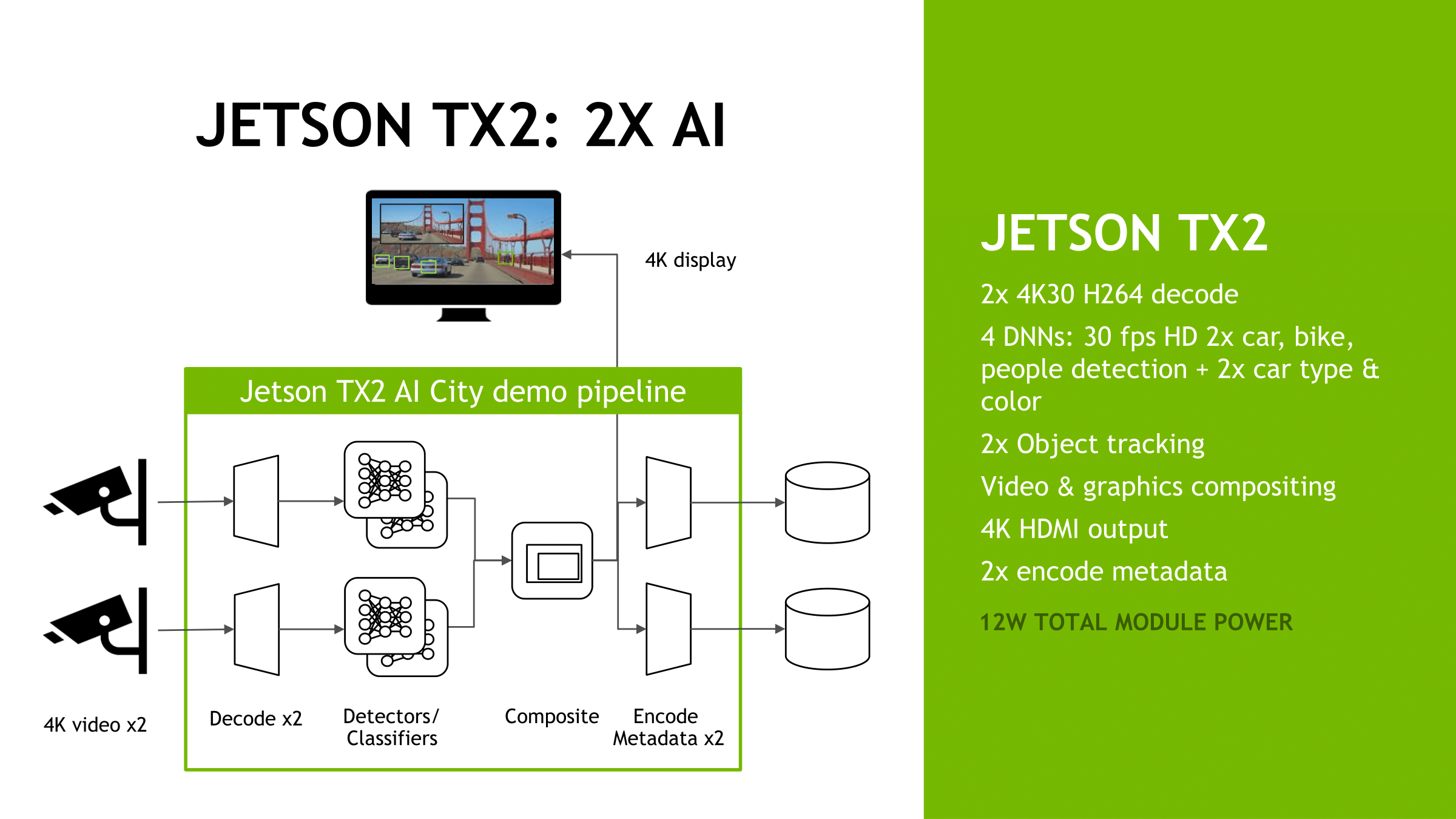
This relaunched Jetson came at an interesting time for NVIDIA, which was right when their fortunes in neural networking/deep learning took off in earnest. Though the Jetson TX1 and underlying Tegra X1 SoC lack the power needed for high-performance use cases – these are after all based on an SoC designed for mobile applications – they have enough power for lower-performance inferencing. As a result, the Jetson TX1 has become an important part of NVIDIA’s neural networking triad, offering their GPU architecture and its various benefits for devices doing inferencing at the “edge” of a system.
Now about a year and a half after the launch of the Jetson TX1, NVIDIA is going to be giving the Jetson platform a significant update in the form of the Jetson TX2. This updated Jetson is not as radical a change as the TX1 before it was – NVIDIA seems to have found a good place in terms of form factor and the platform’s core feature set – but NVIDIA is looking to take what worked with TX1 and further ramp up the performance of the platform.
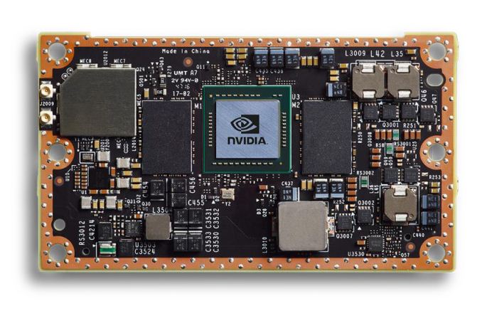
The big change here is the upgrade to NVIDIA’s newest-generation Parker SoC. While Parker never made it into third-party mobile designs, NVIDIA has been leveraging it internally for the Drive system and other projects, and now it will finally become the heart of the Jetson platform as well. Relative to the Tegra X1 in the previous Jetson, Parker is a bigger and better version of the SoC. The GPU architecture is upgraded to NVIDIA’s latest-generation Pascal architecture, and on the CPU side NVIDIA adds a pair of Denver 2 CPU cores to the existing quad-core Cortex-A57 cluster. Equally important, Parker finally goes back to a 128-bit memory bus, greatly boosting the memory bandwidth available to the SoC. The resulting SoC is fabbed on TSMC’s 16nm FinFET process, giving NVIDIA a much-welcomed improvement in power efficiency.
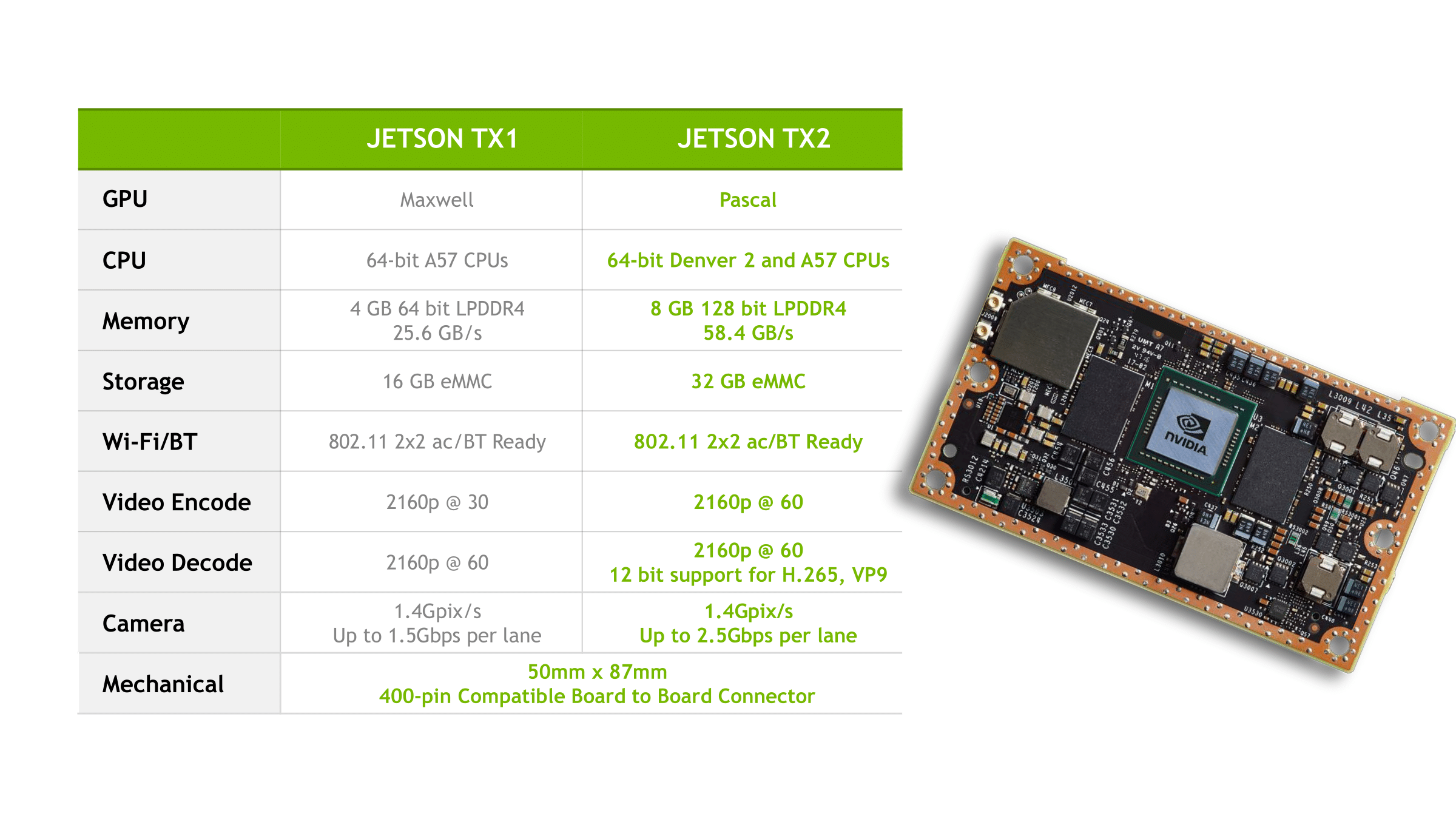
Paired with Parker on the Jetson TX2 as supporting hardware is 8GB of LPDDR4-3733 DRAM, a 32GB eMMC flash module, a 2x2 802.11ac + Bluetooth wireless radio, and a Gigabit Ethernet controller. The resulting board is still 50mm x 87mm in size, with NVIDIA intending it to be drop-in compatible with Jetson TX1.
Given these upgrades to the core hardware, unsurprisingly NVIDIA’s primary marketing angle with the Jetson TX2 is on its performance relative to the TX1. In a bit of a departure from the TX1, NVIDIA is canonizing two performance modes on the TX2: Max-Q and Max-P. Max-Q is the company’s name for TX2’s energy efficiency mode; at 7.5W, this mode clocks the Parker SoC for efficiency over performance – essentially placing it right before the bend in the power/performance curve – with NVIDIA claiming that this mode offers 2x the energy efficiency of the Jetson TX1. In this mode, TX2 should have similar performance to TX1 in the latter's max performance mode.
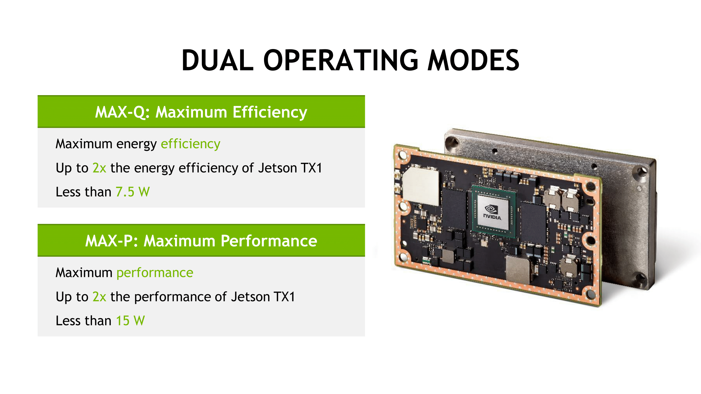
Meanwhile the board’s Max-P mode is its maximum performance mode. In this mode NVIDIA sets the board TDP to 15W, allowing the TX2 to hit higher performance at the cost of some energy efficiency. NVIDIA claims that Max-P offers up to 2x the performance of the Jetson TX1, though as GPU clockspeeds aren't double TX1's, it's going to be a bit more sensitive on an application-by-application basis.
| NVIDIA Jetson TX2 Performance Modes | |||||
| Max-Q | Max-P | Max Clocks | |||
| GPU Frequency | 854MHz | 1122MHz | 1302MHz | ||
| Cortex-A57 Frequency | 1.2GHz | Stand-Alone: 2GHz w/Denver: 1.4GHz |
2GHz+ | ||
| Denver 2 Frequency | N/A | Stand-Alone: 2GHz w/A57: 1.4GHz |
2GHz | ||
| TDP | 7.5W | 15W | N/A | ||
In terms of clockspeeds, NVIDIA has disclosed that in Max-Q mode, the GPU is clocked at 854MHz while the Cortex-A57 cluster is at 1.2GHz. Going to Max-P increases the GPU clockspeed further to 1122MHz, and allows for multiple CPU options; either the Cortex-A57 cluster or Denver 2 cluster can be run at 2GHz, or both can be run at 1.4GHz. Though when it comes to all-out performance, even Max-P mode is below the TX2's limits; the GPU clock can top out at just over 1300MHz and CPU clocks can reach 2GHz or better. Power states are configurable, so customers can dial in the TDPs and desired clockspeeds they want, however NVIDIA notes that using the maximum clocks goes further outside of the Parker SoC’s efficiency range.
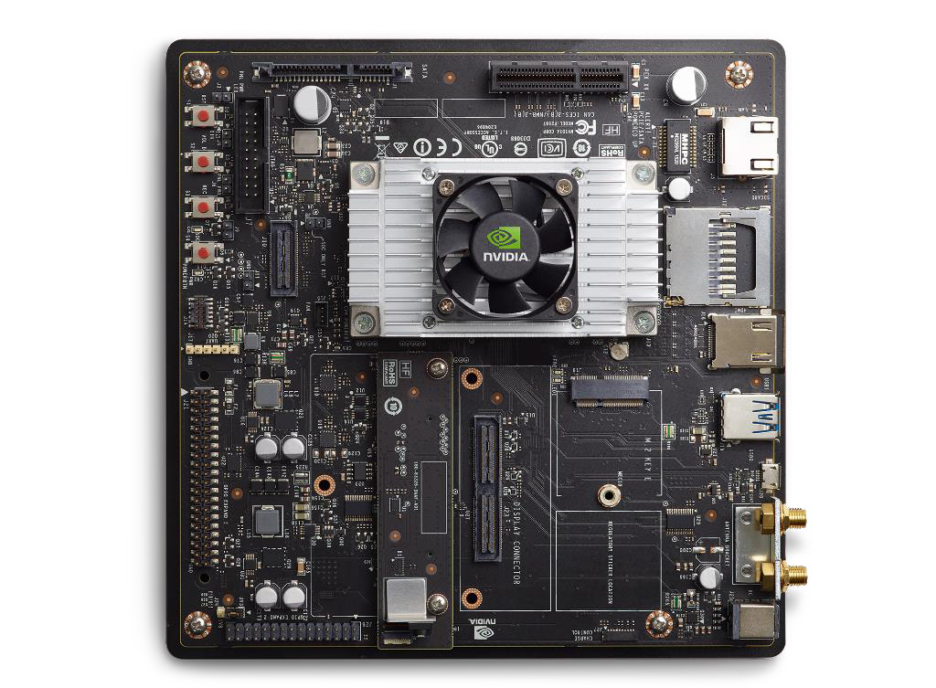
Finally, along with announcing the Jetson TX2 module itself, NVIDIA is also announcing a Jetson TX2 development kit. The dev kit will actually ship first – it ships next week in the US and Europe, with other regions in April – and contains a TX2 module along with a carrier board to provide I/O breakout and interfaces to various features such as the USB, HDMI, and Ethernet. Judging from the pictures NVIDIA has sent over, the TX2 carrier board is very similar (if not identical) to the TX1 carrier board, so like the TX2 itself is should be familiar to existing Jetson developers.
With the dev kit leading the charge for Jetson TX2, NVIDIA will be selling it for $599 retail/$299 education, the same price the Jetson TX1 dev kit launched at back in 2015. Meanwhile the stand-alone Jetson TX2 module will be arriving in Q2’17, priced at $399 in 1K unit quantities. In the case of the module, this means prices have gone up a bit since the last generation; the TX2 is hitting the market at $100 higher than where the TX1 launched.


Source: NVIDIA


59 Comments
View All Comments
ddriver - Tuesday, March 7, 2017 - link
Once again - too expensive. Even more "too expensive" than the previous one. Not that there can be a direct comparison between market niches, but for that amount of money you can get a x86 itx board with a quad core i7, 16 gigs of ram and a decent gpu.Other vendors sell dev/eval boards below their actual value in order to hook up OEMs to use the platform in their products, and then there is nvidia, too big (or small) to miss on the opportunity to rake in profits on something as limited in volume as dev boards.
Way to go nvidia, I mean winning designs for a chip that costs like 15$ to make and sells at 400$ to OEMs... That would actually explain why nvidia socs are nowhere to be found in consumer products.
jordanclock - Tuesday, March 7, 2017 - link
Will that ITX i7 system use 15 watts?ddriver - Tuesday, March 7, 2017 - link
You appear to have missed the "Not that there can be a direct comparison between market niches" part.BTW this product is marketed for automotive. Not mobile phones or tablets, where battery life is critical. Vehicles which have kilowatts of power at their disposal, which would have no problems running more power hungry platform.
So while an i7 itx platform would probably not use 15 watts, it will offer much better performance and value for the price and power consumption. And being more power hungry would not be detrimental if you put it in a car. So no, fitting in a 15 watt power budget is not a big whoop, and certainly doesn't justify the ridiculous price.
Meteor2 - Wednesday, March 8, 2017 - link
So why make your comparison, if you admit it's not possible?By all accounts there's a market for this board; it is being purchased and it is being used. That suggests the pricing is correct. If it were cheaper it would likely not leave enough margin for future R&D to continue moving the state of the art onwards.
Vatharian - Wednesday, March 8, 2017 - link
Where you're wrong, that there is no direct comparison. There is in form of Atom boards, but they're a bit underpowered. But then again, there is literally copetitor in form of Intel Gordon Ridge, which is nearly ready made into automotive format, with ready-to-install kits.And even there, i7, or really any architecture beyond Haswell easily scales from 217 to 1.3W, even on same chip.
As long as you can create robust silicon with abundance of GPIO/can and decent software, anything is open game.
Also main limitation of automotive isn't power (which is important in standby, by the way, no one likes to discover that your car battery has gone flat in a week you haven't been driving your vechicle), but cooling. Leaving a car in 50°C/120°F for a day shouldn't damage the thing.
hecksagon - Wednesday, March 8, 2017 - link
Power isn't a problem in automotive, what is a problem is heat. In automotive you have to validate a design for every conceivable environment. This includes days of -40°F and 120° temperatures, with a hot engine running and limited airflow inside the dash. You think a desktop i7 is going to run in a cramped dash with no airflow? Is it going to last for the life of the vehicle? The nVidia solution is much better because it keeps the TDP low, performance relatively high, has soldered components, and may even require no active cooling in production versions. That removes or mitigates dozens of failure modes.extide - Sunday, March 12, 2017 - link
There is always this: http://www.anandtech.com/show/11052/asrock-shows-d... -- ITX w/MXM -- so you can put a 35W i7 in there with a 1080 MXM...extide - Sunday, March 12, 2017 - link
Sorry, MicroSTX, so even smaller...BertrandsBox - Tuesday, March 7, 2017 - link
This isn't for your everyday computing. It's not meant for tablets, desktops, or anything of that sort. This is specifically developed for 'edge cases' in AI where it becomes desirable to shift processing on-location and not be constantly sending data back and forth to a data center to make sense of anything.Your example of an x86 board, with a quad core i7, 16 GB of RAM, and a 'decent' GPU would take up at a minimum, ~6.64 times more space (assuming mini-ITX), consume untold times more energy, and certainly isn't going to fit in anything like a traffic cam, like this is designed for.
I'm gonna have to assume you're trolling, because even there's no way anybody would write such an asinine comment without doing it on purpose.
ddriver - Tuesday, March 7, 2017 - link
I am going to assume you are an nvidia fanboy, who has never seen an itx board in real life, because if you had you'd realize it is not that much bigger than this dev board. And judging by laptop mobos, i7 can fit into much smaller spaces and into much more modest power budgets. Amazing, I know.Untold times more energy? Maybe numbers beyond 4 boggle your mind too? There is no magic to this, it is not intrinsically superior, the computing performance it delivers is in line with the power it consumers. A vega based gpu has 25 tflops of fp16 throughput at below 250 watts, meaning less than 10 watts per tflop, whereas this thing gets its tflop at 15 watts, while costing as much as solution that is 25 times more powerful. You mean to tell me that if amd were to chop off 1/25th of a vega to get a solution that does 1 tflop per 10 watts of power budget, that would be such an achievement that it will justify asking the same price for this 1/25th as for the 25 times more powerful solution?
It is not a miracle product. It's power requirements are well in line with the performance it offers. It consumers little power because it doesn't have too many transistors and it doesn't offer that much performance. Its power requirements do not justify its ridiculous cost. It should cost like 50 bucks for the module, 75 for the dev board.