AMD Reveals More Llano Details at ISSCC: 32nm, Power Gating, 4-cores, Turbo?
by Anand Lal Shimpi on February 8, 2010 12:00 AM EST- Posted in
- CPUs
After cashing Intel’s check and appearing more competitive than expected against Clarkdale 2010 is like a fresh start for AMD. The news gets better.
Late last year AMD said that before the end of 2010 it would be sampling its first APU (Accelerated Processing Unit) - codenamed Llano. Today AMD is announcing that the first Llano samples, built on Global Foundries 32nm high-k + metal gate, SOI process will be sampling to partners in the first half of this year.
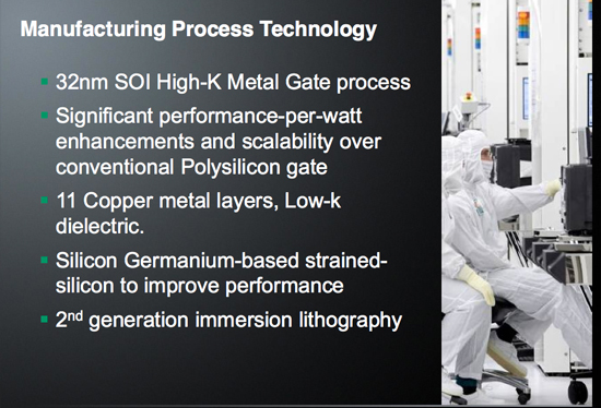
GF's 32nm SOI High-K + MG process will be used with Llano
For those not in the know, Llano is AMD’s first hybrid CPU-GPU with on-die graphics. The graphics core is a derivative of AMD’s DirectX 11 Evergreen lineup (the same lineage as the Radeon HD 5970, 5870, 5850, 5670, 5570, 5450, etc...).
Llano will go up against Sandy Bridge, which seems to have been pushed back to 2011 for volume availability according to Intel’s internal roadmaps. While Sandy Bridge will have graphics on-die, it will still only be DX10 class - AMD will have the feature-set advantage as far as graphics is concerned.
Llano's Features
Today we learn a bit more about the CPU side of Llano. The first chip will be a quad-core processor plus on-die graphics. Each core is Phenom II derived, but there’s no shared L3 cache. So Llano cores look a lot like Athlon II cores. I’m hearing that they may have some architectural tweaks, so performance could be better than present-day Athlon IIs.
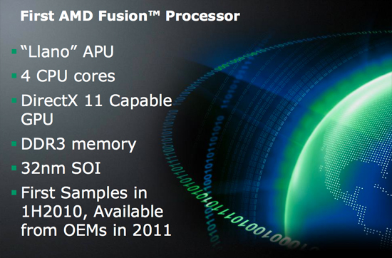
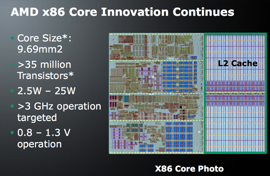
At 32nm each core (minus L2 cache) is only 9.69 mm^2 and is made up of over 35M transistors. Each core is paired with its own 1MB L2 cache, meaning the quad-core processor will have a total of 4MB of L2 on-die. AMD expects Llano to run at above 3GHz, which should be more than possible at 32nm given that we’re already at close to 3GHz with the 45nm Athlon II X4.
AMD’s First Power Gated CPU
With Nehalem Intel introduced power gating, a technique that allows a core to be near-completely powered down minimizing leakage current when inactive. This not only reduces idle power but it also enables Intel to use extra TDP to turbo up active cores.
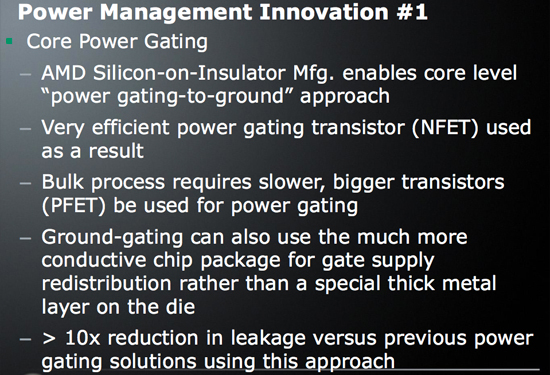
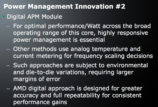
Llano uses power gating as well as a Digital APM Module. AMD doesn’t go into much detail on the digital APM module but I’m guessing we’ll see the same sort of turbo-like functionality out of Llano, including graphics turbo.
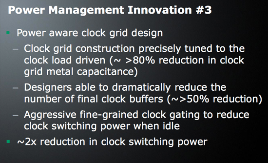
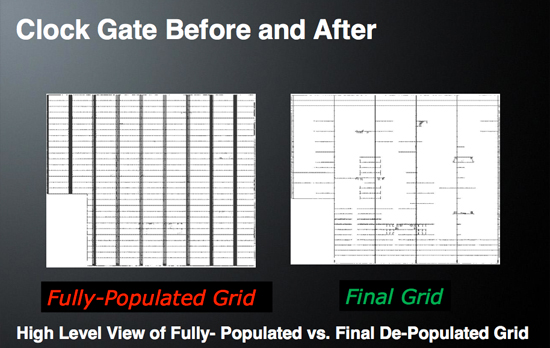
AMD also pointed out that Llano uses a “power aware clock grid design”. I couldn’t get much more information out of AMD on this one, other than its expecting a ~2x reduction in clock switching power. Simply distributing the clock to all parts of a modern day microprocessor can take up quite a bit of power, any improvements in efficiency there are very important.
I’ll keep digging to see if I can get any more details on this aspect of Llano.
Final Words
Llano will obviously require a new socket. All AMD is saying is that OEMs will be shipping systems in 2011. It’s unclear if we’ll see anything in the channel before then, but with sampling in the coming months it appears that AMD could be ready for Sandy Bridge when it arrives next year.
AMD isn’t qualifying its 2011 statement with an indication of what quarter to expect systems. Given that the first samples are going out now, I’d expect to see Llano sometime in the first half of 2011 but that’s purely conjecture on my part. Sandy Bridge is scheduled to ship in volume in the first quarter of 2011.
The big questions going forward are 1) how much AMD and Intel are going to scale up its graphics performance on these chips, and 2) how important DX11 support will be to the upcoming APU race.


58 Comments
View All Comments
kenyee - Tuesday, February 9, 2010 - link
Intel has some cool features like virtual port assignment, etc. that AMD currently doesn't have (so databases and gigabit network cards go faster on Intel VT hardware in the upper end Xeons).Does the new AMD core have any improvements in this?
mino - Saturday, February 13, 2010 - link
No.AMD does not produce NIC chips. Go ask Broadcom about that. It a pure NIC feature.
yanfei - Sunday, July 25, 2010 - link
======= http://www.fashionshoppong.us=======haplo602 - Tuesday, February 9, 2010 - link
I think I recall that AMD expects the GPU to take the most of the FPU load in the future, so maybe the APU chip will be an FP op monster when the GPU part is not used much. Pair that with an external GPU and theoreticaly unused on die GPU in AM3 and there is actualy no problem for AMD to make the chip AM3 compatible..Anyway I don't give a damn about Direct Compute whatever version it is. I want good OpenCL performance and finaly decent OpenGL drivers from ADM. And finaly a working and usable Linux driver would be nice.
mjw25a - Wednesday, February 10, 2010 - link
Correct, worth taking a look at http://tech.icrontic.com/articles/amd-in-2010-part...">http://tech.icrontic.com/articles/amd-in-2010-part...If there's sone thing interesting about the two next generation (Bulldozer and Bobcat)architures (modules) it's that they both appear to have been designed with far less floating point power than previous AMD CPU's.
This tends to indicate that both next gen modules will likely have a GPU on the same die to shunt floating point operations to.
Traditionally GPU's completely smash the x86 architecture when it comes to floating point performance so this will be a good move.
The Llano looks to be a the use of the current gen Propus (Athlon II) core with an APU to massively boost floating point performance.
Not a big deal as it looks like they're positioning Llano as their mainstream product whereas Bulldozer will fit into the same niche as the i7 is currently in. Bobcat is their atom equivalent which should beat that handily.
I'll be keenly watching the renewed CPU wars next year. This integration of the GPU has the potential for AMD to leapfrog Intel in all performance segments if they can pull it off. Intel's graphics chips so far have been abysmal.
The Larabee will not help them in this respect as it's essentially a large grid of dumbed down x86 cores. As I've previously mentioned, floating point operations have always been x86's weakness.
Next year will be interesting indeed.
hwhacker - Tuesday, February 9, 2010 - link
We pretty much already know from the die shot the 'APU' is 480sp, which implies 8 ROP and 24 TMU. A little stronger than 5670 architecturally speaking.GF has said 28nm bulk should allow for a 40% increase in clock speed compared to the same size die and TDP of a 40nm bulk chip, and 28nm is a 10% linear shrink of 32nm. Of course SOI should have better characteristics than bulk, but that gives you an idea of what to expect. Because of the given die size of the core minus L2 in the article, we now know Fusion is 13x13mm2, 169mm2, or exactly the same size as Propus (Athlon II X4), so THIS DOES APPLY.
Imagine a very possible scenario where the GPU is clocked at 1/4 of the CPU standard. It's very plausible this could start at the 3.2-3.6ghz (800-900mhz gpu) and creep up to 4ghz with a 1ghz GPU clock contained in a 95W TDP. Wouldn't be surprised by an ~875mhz set clock either.
Add to that the probability of Sideport going to two chips instead of one. When the 900 series chipset(s) launches, GDDR5 will be in 2Gb form. This means a likely 512MB of decent on-board memory, perhaps of the 7Gbps variety. That's 56Gbps on a 64-bit bus.
What we'll likely end up with is a GPU that will be faster than an 8800gt, sometimes by a lot, slower than 5750/gts250, likely questioning the usefulness of a 128sp 64-bit 28nm Fermi for either platform, and perhaps a xfire partner to the smallest Northern Island. This also brings the defacto standard for gaming to this level, which is GREAT news, because lots of people own old 8800gt or similar-performing cards as hand-me-downs.
On the CPU side, just simply compare Athlon X4 to Clarkdale. I would imagine the 2c version of Sandy Bridge is essentially Clarkdale with GPU on die, with similar cpu clockspeeds, tdp, and die size to fusion. That would mesh with the 4c die shot that's been on the net for 6 months (Citing 3-3.8ghz clocks and 1-1.4ghz gpu). The thing is, AMD will have a CAPABLE gpu.
Personally, I think it's going to be cake-and-eat-it for anyone gaming below 1680x1050 at that point, say a 720/768p htpc, or a good casual all-arounder + GPGPU perks. Plus, If you look at a 5670, there's plenty of stuff it can run at decent rez...This could be up to a third faster in some cases, if such speculation pans out.
tcube - Saturday, March 20, 2010 - link
Your asumption that the gpu will not have the same clock as the cpu is kind of odd to say the least... It's the same(exactly the same) process as the cpu why on earth would you want to have it artifically downclocked? Since a) soi is much more efficient and dense and b) you're working on a smaller node with much better technology with much less heatdissipation and so on... The 2 things aren't even 2 dies like in the intel solution ... they are on the same friggin silicon... If it will feature 480 sp's @ 3+ GHz it would behave as a ~1600 sp bulk gpu (eerm... remember HD5870...) so what's the deal? Plus think of all the v/frequency synch you need to do between the 2 cores to get them in one line... Why even bother with all that if you can put a gpu+cpu on a silicon that can outrun any current generation laptop solution at far less power drain??LeftSide - Wednesday, September 1, 2010 - link
I don't think you understand the difference between GPUs and CPUs. Because of the way they are designed CPUs clock higher. This has to do with the pipeline in a CPU. Ever wonder why the highest clocked Pentium 4 still runs faster than the fastest i7?iamezza - Tuesday, February 9, 2010 - link
no way the GPU would be THAT fast. It would completely destroy ATI sales.Am1R - Thursday, February 11, 2010 - link
well by that time Ati discrete GPU will be twice as fast