AMD Opteron Coverage - Part 1: Intro to Opteron/K8 Architecture
by Anand Lal Shimpi on April 23, 2003 3:03 AM EST- Posted in
- CPUs
Let's get physical
Thus far we've focused on the core architecture of the Opteron, but there's much more to a CPU than the microarchitecture.
The Opteron is built on AMD's most advanced manufacturing process to date - a 0.13-micron process featuring Silicon on Insulator (SOI). Additional frequency headroom and cool running operation are both positive benefits of SOI, for more information on what SOI is be sure to read our quick one-page explanation of it here.
Thanks to its 1MB L2 cache on top of its already complicated die, the Opteron is AMD's biggest and most expensive chip to manufacture - with a die measuring just under 200 mm^2. AMD has told us in the past that their manufacturing sweet spot is around the 100 - 120mm^2 mark; it's clear that AMD isn't having much fun making Opteron.
The expensive chip continues to be a nuisance to manufacture once you look at the underside of the CPU, at all 940 pins. The packaging costs alone are higher than anything AMD is used to, thanks to the three HT links and 128-bit wide memory interface present on every Opteron CPU (this partially explains the very high pricetag of Opteron processors).
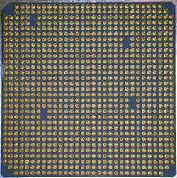
Interestingly enough, AMD has reverted back to using a ceramic package with the Opteron rather than the organic packaging introduced with the Athlon XP. AMD will certainly have to migrate to organic packaging as clock speeds increase, but we have a feeling that the benefit of reduced current draw courtesy of SOI has enabled AMD to stick with a ceramic packaging where they couldn't otherwise.


1 Comments
View All Comments
skunklet - Thursday, June 30, 2005 - link
YEAH