The Huawei Mate 8 Review
by Andrei Frumusanu on January 5, 2016 1:00 PM EST- Posted in
- Mobile
- Smartphones
- Huawei
- Cortex A72
- Kirin 950
- Mate 8
- CES 2016
GPU Performance
In terms of GPU we see the first implementation of ARM’s new Mali T880 GPU in a 4-cluster configuration running at up to 900MHz. In terms of performance improvements ARM’s isn’t as clear what the actual benefits of the new Mali T860 is compared to the previous generation T760, but we do know that the T880 has the distinct improvement of coming with 3 instead of 2 ALU pipelines per GPU cluster, representing a 50% increase in theoretical computational power. Together with the high 900MHz operating clock of the Kirin 950 and introduction of LPDDR4 memory running at 1333MHz, we should see solid improvements over past high-end Kirin SoCs although HiSilicon is still being conservative in the GPU configuration as the MP4 implementation in the Kirin 950 is rather small compared to for example what we’ve seen from Samsung’s Exynos chipsets.
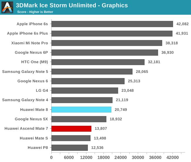
Starting with 3DMark Ice Storm Unlimited we see that the Mate 8 is able to show a good improvement over past Kirin SoCs but can’t keep up with the more performant GPUs from Qualcomm and Samsung.
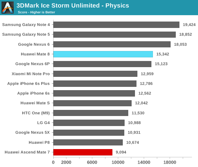
The physics test shows some very good improvements as the test stresses both GPU and CPU.
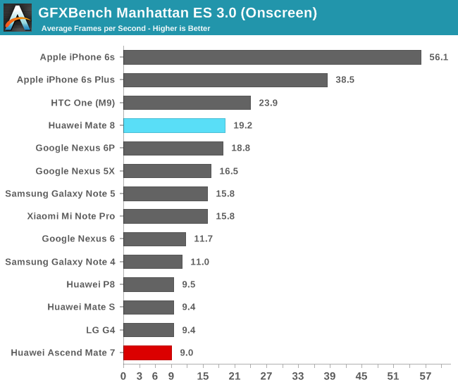
Kishonti’s GFXBench Manhattan sees a doubling of the framerate from 9.5 to 19.2fps. This is interesting as it means the new GPU is able to take advantage of its architectural advancements to improve performance per clock compared to the Mali T628. The difference is quite large, but unfortunately we won’t be able to better analyse just how much the new GPU improves over its predecessors until we are able to get better control over the platform’s drivers to be able to test it in the same way we investigated the Mali T760 in last year’s Exynos 5433.
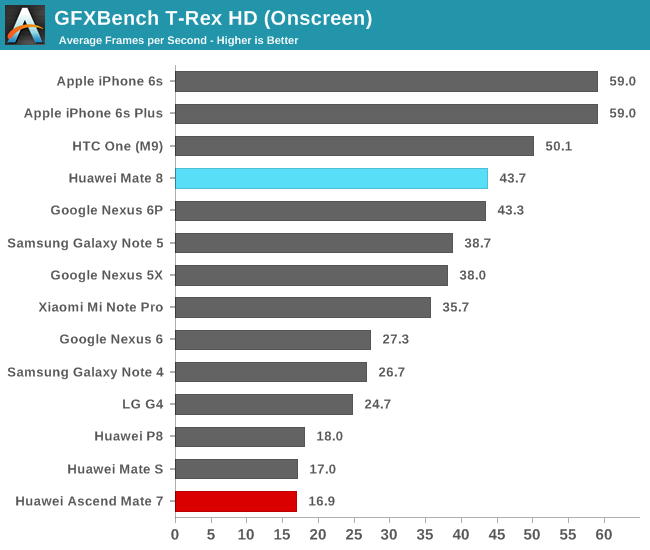
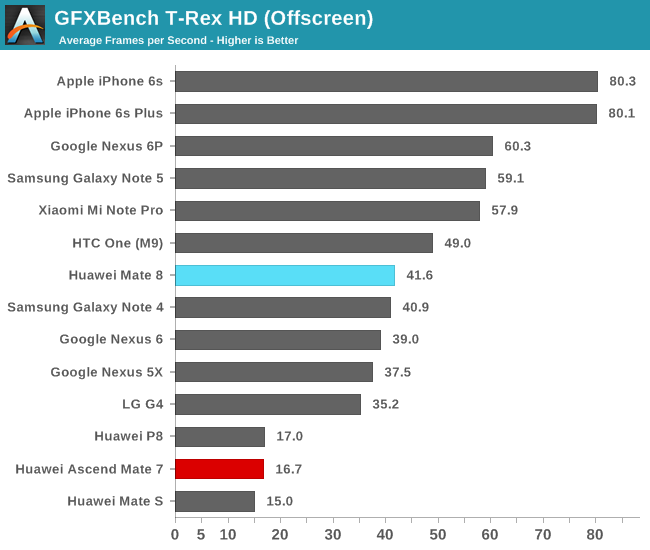
The on-screen T-Rex tests show an even larger performance improvement as we’re getting 2.5x the performance of the T628 in the Kirin 925 and 935. The 220MHz (32%) clock advantage alone isn’t able to account for the performance increase and the remaining factors coming from the addition of a new LPDDR4 memory controller are also far greater than what we’ve seen from the T760, leaving us with the only viable explanation that ARM’s new GPU generation is able to show some solid improvements in terms of performance at the same clock and physical configuration.
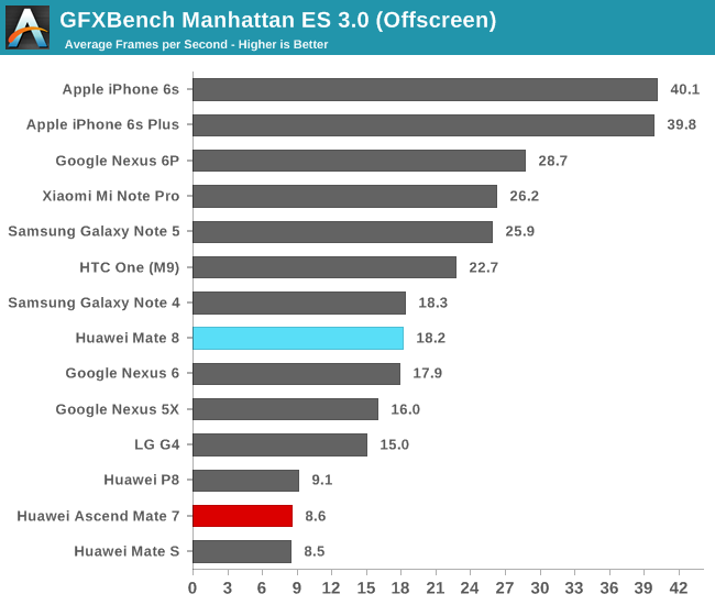
In the off-screen tests we see similar scaling improvements of the Mali GPU in the Kirin 950, but now we see a more apples-to-apples comparison between it and the competition. It looks like Kirin 950’s configuration lands it at a similar performance level as the Adreno 420 found in last year’s Snapdragon 805 devices.
3D Power
As we’ve hopefully come to learn over the past year, raw performance is not the only factor that determines how good a device is in gaming, but also what kind of power levels the phone is able to sustain and what kind of total efficiency level the SoC + platform are able to deliver.
We continue to make usage of Kishonti’s GFXBench T-Rex and Manhattan tests to determine the efficiency levels of the current generation of GPUs.
| T-Rex Offscreen Power Efficiency (System Load Power) |
||||||
| Mfc. Process |
FPS | Avg. Power | Perf/W Efficiency |
|||
| Snapdragon 810v2.1 (Mi Note Pro) | 20SoC | 57.6 | 4.40W | 13.11 fps/W | ||
| Exynos 7420 (S6) | 14LPE | 56.3 | 4.82W | 11.63 fps/W | ||
| Kirin 950 (Mate 8) Est. | 16FF+ | 41.6 | 3.64W | 11.40 fps/W | ||
| Snapdragon 805 (S5LTEA) | 28HPM | 40.7 | 4.06W | 10.02 fps/W | ||
| MT6595 (MX4) | 28HPM | 23.3 | 2.42W | 9.55 fps/W | ||
| Snapdragon 810v2.0 (G Flex2) | 20SoC | 45.5 | 4.84W | 9.39 fps/W | ||
| Exynos 5430 (MX4Pro) | 20LPE | 28.7 | 3.55W | 8.08 fps/W | ||
| Snapdragon 801 (S5) | 28HPM | 26.9 | 3.47W | 7.77 fps/W | ||
| Exynos 5433 (Note 4) | 20LPE | 37.3 | 5.35W | 6.97 fps/W | ||
| Exynos 5430 (Alpha) | 20LPE | 31.3 | 4.88W | 6.41 fps/W | ||
| Kirin 935 (Mate S) Est. | 28HPM | 16.7 | 3.17W | 5.26 fps/W | ||
| Kirin 925 (Mate 7) Est. | 28HPM | 15.8 | 3.29W | 4.79 fps/W | ||
In the T-Rex test we see that the Mate 8 and the Kirin 950 are able show a very reasonable power consumption of around 3.64W at 41.6fps. This results in an efficiency estimated at about 11.40 fps/W, almost on par with the Exynos 7420 in the Galaxy S6. The difference here is that HiSilicon targets a much more sustainable power level at maximum frequency while the latest generation Qualcomm and Samsung SoCs exceed power envelopes that would fit in mobile devices.

An interesting question for the efficiency of the Mali T880 is how it compares to the T760 in the Exynos 7420. Here we’re seeing to different design philosophies as HiSilicon prefers to push for high clocks at narrower GPU configurations while Samsung goes for wider implementations at lower clocks (Although they’re still relatively high at 700+MHz). Here we see that going narrower and clocking higher is a disadvantage as we’re trading off die size for efficiency. At a similar power consumption of 3.36W the Exynos 7420 is able to achieve 45.6 fps for an efficiency of 13.67fps/W, higher than that of the Kirin 950’s even though the latter has a process node and architectural advantage.
| Manhattan 3.0 Offscreen Power Efficiency (System Load Power) |
||||||
| Mfc. Process |
FPS | Avg. Power | Perf/W Efficiency |
|||
| Kirin 950 (Mate 8) Est. | 16FF+ | 18.2 | 3.18W | 5.71 fps/W | ||
| Exynos 7420 (S6) | 14LPE | 24.8 | 4.87W | 5.08 fps/W | ||
| Exynos 5430 (MX4Pro) | 20LPE | 12.3 | 3.20W | 3.84 fps/W | ||
| MT6595 (MX4) | 28HPM | 8.1 | 2.15W | 3.76 fps/W | ||
| Snapdragon 805 (S5LTEA) | 28HPM | 18.2 | 5.20W | 3.66 fps/W | ||
| Snapdragon 810v2.1 (Mi Note Pro) | 20SoC | 27.5 | 7.30W | 3.52 fps/W | ||
| Snapdragon 810v2.0 (G Flex2) | 20SoC | 22.2 | 5.82W | 3.34 fps/W | ||
| Snapdragon 801 (S5) | 28HPM | 11.9 | 3.75W | 3.17 fps/W | ||
| Exynos 5430 (Alpha) | 20LPE | 12.7 | 4.07W | 3.11 fps/W | ||
| Exynos 5433 (Note 4) | 20LPE | 17.5 | 6.08W | 2.87 fps/W | ||
| Kirin 935 (Mate S) Est. | 28HPM | 16.7 | 3.04W | 2.82 fps/W | ||
| Kirin 925 (Mate 7) Est. | 28HPM | 15.8 | 3.13W | 2.54 fps/W | ||
In Manhattan 3.0 we actually see the Kirin 950 beat all other devices in terms of power efficiency. Although the T880 features 50% more ALUs than previous Mali GPUs, the total power is still lower than what we see in T-Rex as it comes at 3.18W. This bodes very well for the T880 as we could see even higher efficiency numbers from wider and lower clocked implementations such as the one in the upcoming Exynos 8890. ARM continues to have a good efficiency advantage over Qualcomm’s Adreno GPUs when it comes to computational heavy workloads. We’ll have to wait a bit more to see how the new Snapdragon 820 and the Adreno 530 fare in this aspect.
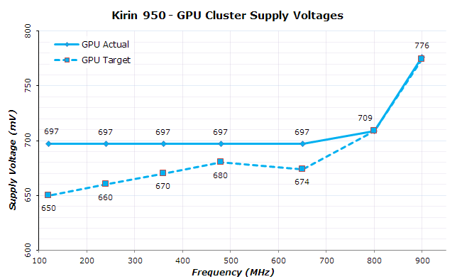
Similar to the A72 cluster, it looks like the GPU cluster is also capped in terms of minimal supply voltage as the GPU stops scaling down after the 650MHz frequency point which is rather unfortunate and means that we’re not seeing the best showing of the SoC as the lower frequencies are the ones most often used in everyday scenarios.
Overall, the Kirin 950 seems to showcase very competitive efficiency at its highest operating points while still maintaining power envelopes that are fit for a smartphone.
Device Thermals
Peak power and power efficiency are what determine the overall sustained performance of a device. In 3D workloads we saw that the Mate 8 and the Kirin 950 are able to show exemplary peak power fitting smartphone phone factors so we should be expecting quite good sustained performance from the Mate 8.
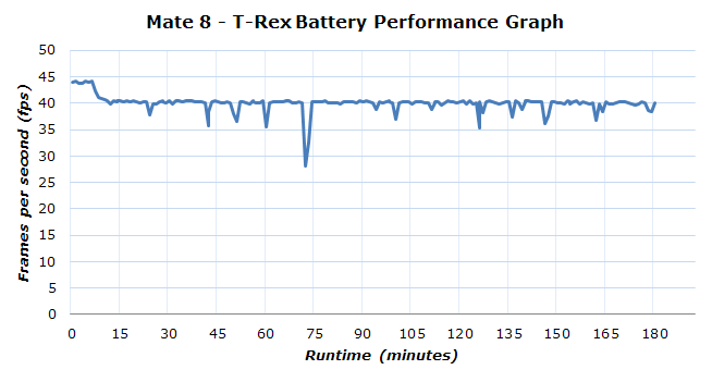
Indeed when looking at the battery rundown test of the Mate 8 we see that it’s able to maintain near peak performance for the whole duration of the run, only throttling down to lower frequencies for small periods of time. This again bodes well for the Kirin 950 as it looks like its GPU configuration is well justified and well balanced. The fact that the Mate 8 only sports a 1080p screen enables the phone to achieve some of the best sustainable performances in games among current Android devices.
A new kind of measurement test that I conjured up for our SoC evaluations and first published in the review of the Nexus 6P was a CPU throttling benchmark. Here I use a CPU power virus with two threads (loading up 2 CPU cores) over a duration of little over 25 minutes. The point of this exercise is to determine long-term performance in comparison to the maximum performance capable of the device. We’re not measuring the work done here but simply want to compare just how usable the overdrive frequencies of each SoC’s CPUs are. As each device features different thermal dissipation characteristics, the results will always vary even if two devices use the same SoC.
Snapdragon 810 :
Snapdragon 808 :
Exynos 7420 :
Now when first looking at the graph of the Mate 8 things might be a bit confusing as it seems there is no data or something is off, but matter of fact is that the Kirin 950 is able to indefinitely (at least in our test conditions) maintain maximum frequency for two CPU cores. This was really baffling for me as I hadn’t expected a device to already break the new test. The device was barely getting luke-warm as other devices in the test can already reach some high skin temperatures over 40°C while being throttled.

Looking back at the presentation slides from HiSilicon during the launch of the Kirin 950 it now makes a lot of sense why the company was able to advertise such a high increase in the sustained performance of the new chipset.
Out of curiosity to see how and when the new chipset would throttle I decided to go ahead and add in another thread. Theoretically based on the power measurements we saw earlier this represents a power figure of about 3050mW for the SoC and around 650mW for the screen and rest of the phone’s components in idle power.
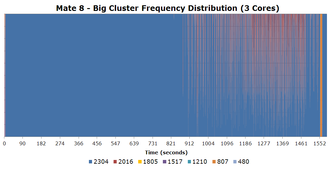
Astoundingly, the Mate 8 and Kirin 950 are able almost also maintain this load for long periods of time as we only see some minor throttling after the 15 minute mark. Here we see that Huawei’s power management is very fine-grained so it should be able to elegantly throttle to more sustainable thermals without much user visible issues.
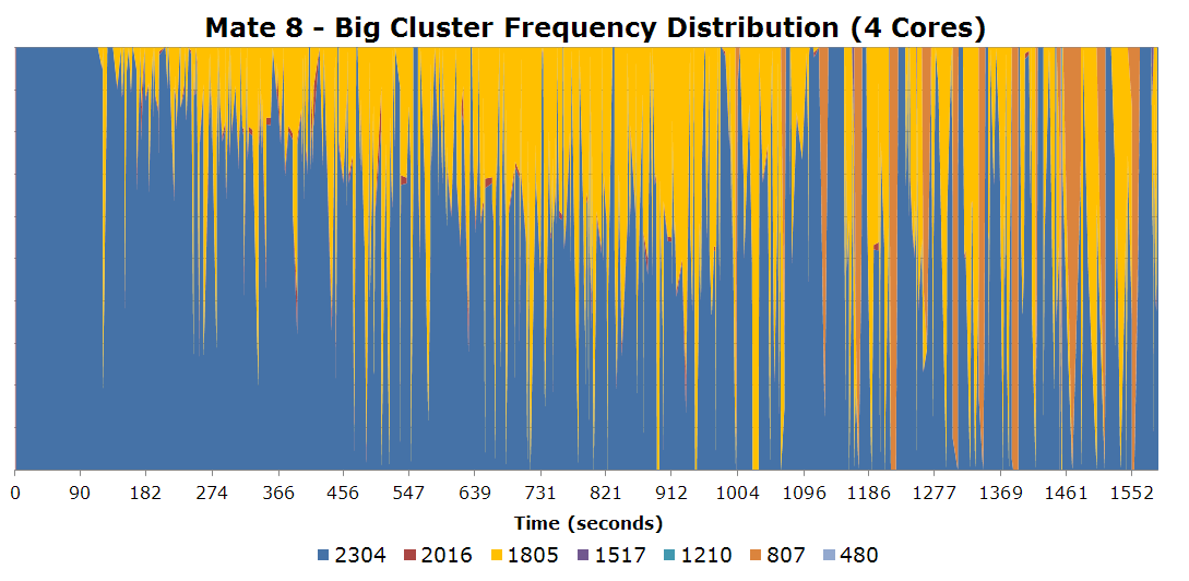
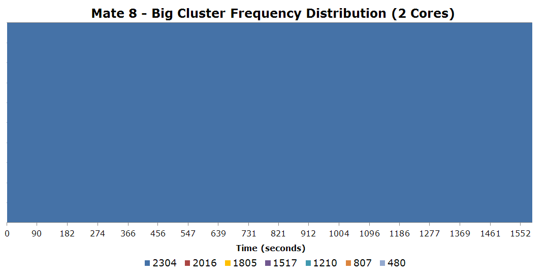
For the sake of completion, I also added in a 4th thread to burn all 4 big CPU cores and better see the throttling behaviour under this test. We’re here seeing the maximum 3.7W CPU EDP under the particular power virus workload we use for testing. The Kirin 950 starts throttling after about 2 minutes as it starts switching between the maximum 2304MHz frequency and the lower 1805MHz state. Towards the end of the test we also see periods of 800MHz – this is because of another thermal protection mechanism. Once the device measures skin temperatures of 43°C it limits the A72 cores to their minimum performance state.
The thermal performance of the Mate 8 is simply exemplary as thanks to the low power consumption of the new Kirin 950 the device is able to enjoy very high sustained performance figures. I hope Huawei is able to continue this trend and that other manufacturers follow suit with SoCs and devices that are able to stay below the magical 3.5-4W peak power figure for both CPU and GPU workloads.


116 Comments
View All Comments
lilmoe - Tuesday, January 5, 2016 - link
CCI (Cache Coherent Interconnect) is basically responsible for connecting and "shifting" load between CPU clusters (, GPU and various other compute blocks) in a big.LITTLE configuration based on compute load needs.For the rest, Google is your friend.
name99 - Tuesday, January 5, 2016 - link
Andrei, do you always use the same compiler, version, and settings for the SPECInt2000 measurements?The reason I ask is if you compare these results to the A9 results
http://www.anandtech.com/show/9686/the-apple-iphon...
things are mostly as you'd expect except 300.twolf and (especially) 175.vpr
The latter in particular is discrepant enough that the only thing that seems like it might have caused it is a substantial compiler optimization like a loop re-ordering.
Andrei Frumusanu - Tuesday, January 5, 2016 - link
On Android we use the same binaries unless we specify some flag changes which happen over longer periods (Last change was in August). Generally we try to publish a given article with apples-to-apples scores.For iOS it's impossible to use the same compilers and we have to rely on Apple's LLVM. It's very possible that Apple's scores are higher due to better optimizations. I have in mind to try LLVM on Android (currently it's GCC) but it's something of a long-term project rather than something we can just switch to and even then it will never solve the optimization issue as Apple's LLVM toolchain has additions that we simply can't keep track of.
name99 - Tuesday, January 5, 2016 - link
To add to my point, compare withhttp://www.anandtech.com/show/9330/exynos-7420-dee...
Here the Exynos 7420 SPECInt2000 numbers are sometimes EXTREMELY different (like sometimes over a factor of 2, eg 175.vpr) from the Exynos 7420 A57 numbers you give in this article.
Maybe it would be good form, going forward, to publish this information, just so we can all keep track. (And obviously it is interesting to see when LLVM results differ greatly from gcc results, or even when the LLVM results show a great jump.)
Obviously one can't hope for PERFECT LLVM parity. Certainly Apple are keeping the back-ends of the compiler toolchain (Typhoon and Twister, maybe even the current Cyclone and Swift back-ends) secret; and given that they use a slightly different linker, there may be differences in exactly how, eg, they handle LTO. But one would expect mostly similarity between the Apple and Android LLVM, and rather more difference with gcc.
My point is not some sort of "rah rah Apple"; it's more just a desire to understand. For example, IS it the case that gcc happens to have some sort of (presumably fairly recent) optimization that managed to double the 175.vpr result? (And if so, what's the nature of that optimization.)
I think we'd all be curious to know, for example, whether you use LTO in building these SPECInt2000 binaries. And whether, if you use PGO, you get a substantial boost in performance.
Andrei Frumusanu - Wednesday, January 6, 2016 - link
There were issues with the 7420 harness that caused us not to immediately catch validation failures and it treated the runtime as if the test were simply faster. SPEC is relatively complex so unfortunately such problems do happen.RdVi - Tuesday, January 5, 2016 - link
Nice improvements from Huawei. If the P9 can keep this up while being no larger than the P8, it might be my next phone.SHartman1976 - Wednesday, January 6, 2016 - link
No complaint about the power and volume buttons being on the same side? That seemed to vex you on the Nexus 6P a couple of weeks ago despite it being a recurring design choice.Andrei Frumusanu - Wednesday, January 6, 2016 - link
My complaint on the 6P wasn't them being on the same side, it was that the volume buttons were extremely low on the phone and positioned below the power button, an odd positioning that kept one pressing the volume buttons when holding or picking up the phone. The Mate 8 has a traditional layout which doesn't cause any issues.raghwendra123 - Wednesday, January 6, 2016 - link
When should we expect the iPad Pro review?Piscupescu - Wednesday, January 6, 2016 - link
Nice review. Keep up the good work.