AMD To Spin-Off Back-End Testing & Assembly Operations Into Joint Venture For $371 Million
by Ryan Smith on October 15, 2015 6:05 PM EST
AMD’s Q3 2015 earnings release just hit the wire a bit ago, and while we’re still working on putting together that story we wanted to immediately jump into what is the biggest news to come out of today’s release. As part of their wave of news releases this afternoon, AMD is announcing that they will be spinning off their back-end manufacturing operations into a new joint venture with Nantong Fujitsu Microelectronics (NFME), with NFME essentially buying the bulk of these operations off of AMD.
Briefly then, in the world of semiconductor manufacturing the complete process of creating a chip is divided into two halves. There is the front-end manufacturing step where a complete wafer of chips is fabbed, and the back-end manufacturing step where those finished wafers are tested and cut up into individual chips for customer use. Dubbed ATMP – for assembly, test, mark, and pack – these back-end operations are in modern times split up from the fabbing step for cost reasons. Consequently capital-intensive and technologically advanced fabbing process will take place in facilities like TSMC Taiwan, GlobalFoundries Germany, and Intel US, while ATMP takes place at facilities in China, Malaysia, and Vietnam.
Up until their spin-off of GlobalFoundries in 2009, AMD had a complete chip manufacturing operation, including facilities for both the fabbing and ATMP operations. Even after the spin-off however, AMD held on to their ATMP operations. It is these operations that AMD is now spinning-off as well, as the company pursues an operations strategy more befitting of a fabless semiconductor designer.
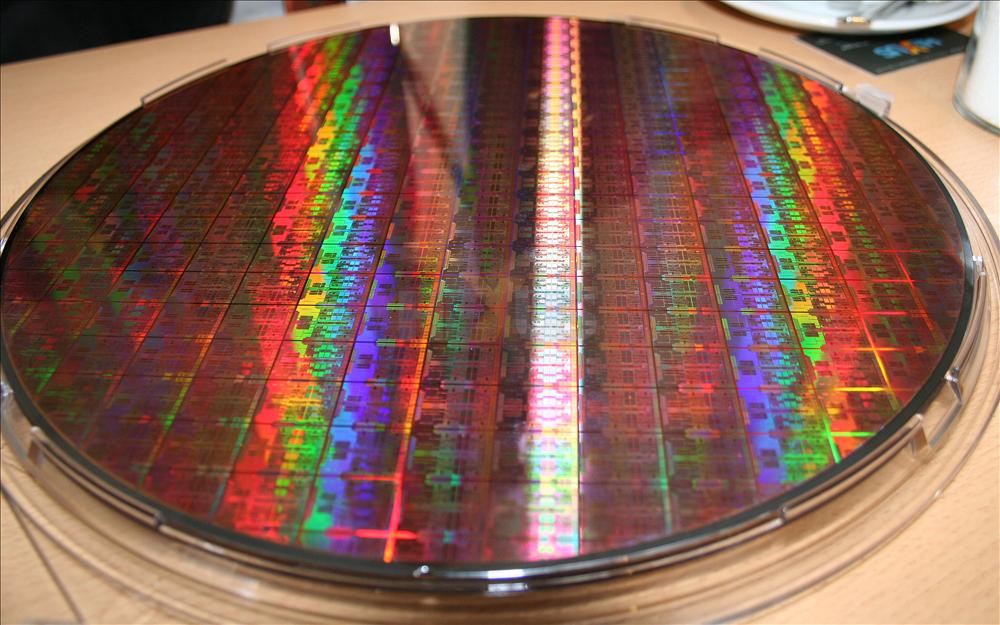
An AMD CPU Wafer (Image Courtesy Hexus.net)
For the deal with NFME, AMD will be spinning-off their ATMP operations into a new, unnamed joint venture in partnership with NFME. The joint venture will see AMD contribute their ATMP facilities in Penang, Malaysia and Suzhou, China, along with their roughly 1,700 person ATMP staff. Meanwhile, though not mentioned in the release, NFME will be contributing their own facilities and employees as well, with the complete joint venture set to have 5,800 employees spread over five facilities.
On the financial side of matters, NFME will immediately be buying an 85% stake of AMD’s ATMP operations, putting NFME in control of the overall joint venture while AMD serves as the minority partner with their remaining 15% share. In turn, NFME will be paying AMD approximately $371 million, and after taxes and other costs this will be a net gain of about $320 million for AMD.
Overall AMD is touting this as a beneficial change for the company, though they also don’t attempt to hide their current financial state in the announcement, stating that the joint venture and sale “further strengthens our balance sheet with significant asset monetization.” AMD on the whole has been struggling with a series of losses over what has now been a number of years, and it has taken a toll on their cash reserves. In the last few years the company has been slowly selling off non-essential or legacy assets in order to both contain ongoing costs and to raise much-needed cash for day-to-day operations. This, among other things, has included selling off and then leasing back their “Lone Star” campus in Austin, Texas.
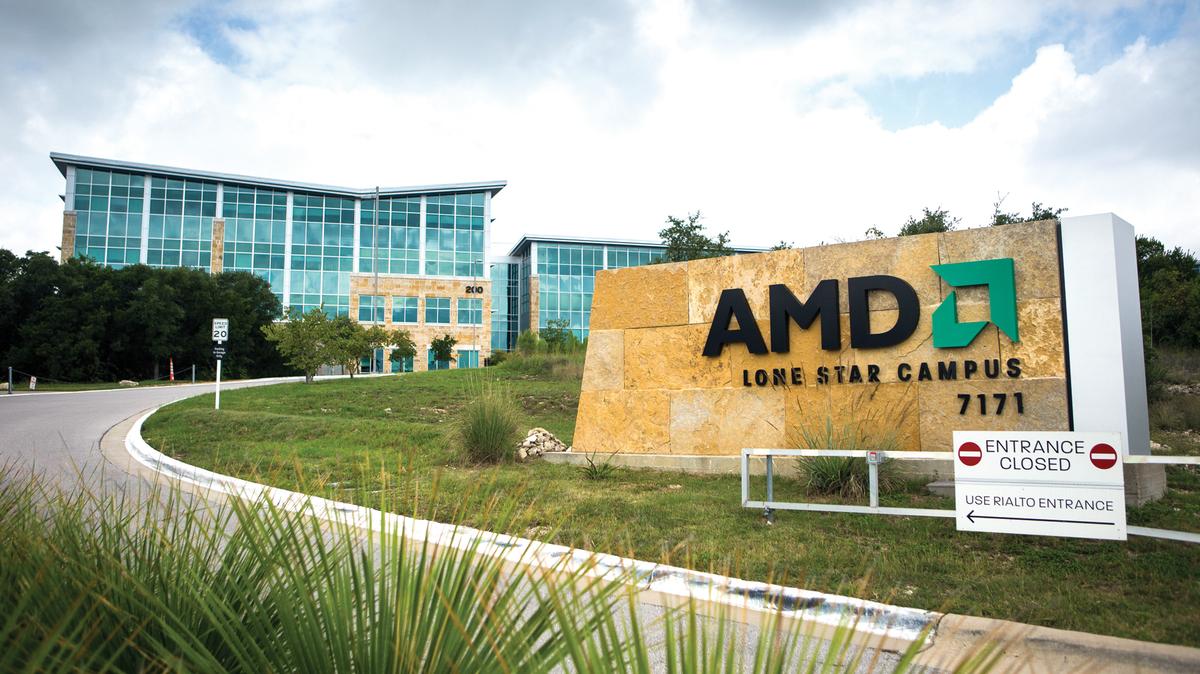
AMD's Leased Lone Star Campus (Image Courtesy Austin Business Journal)
For AMD, the spin-off means they will be removing 1,700 employees from their payroll, which would put their adjusted headcount at around 7,500 to 8,000 employees after the deal closes. Furthermore as ATMP is capital-intensive, this allows AMD to further contain their spending on capital expenditures. AMD has until now held on to their ATMP operations, and at the time of the GlobalFoundries deal stated that they were keeping these operations as they were specifically tailored to AMD’s microprocessor business. However there’s no doubt that the have been an increasing drag on AMD as the company’s revenues and chip volume have continued to shrink. Ultimately as AMD was already fabless, it’s rare to see a fabless company with their own back-end operations anyhow, and AMD believes they can continue to meet their ATMP needs through this joint venture.
As for the joint venture itself, this gives NFME the ability to further expand into the market for semiconductor assembly and test services (SATS). With AMD’s lower product volumes no doubt making it harder to fully utilize their high-volume AMTP facilities, a joint venture with NFME can bring more work into those facilities by having them work for additional customers beyond AMD. Furthermore NVME also gains the R&D experience that comes with AMD’s AMTP operations, which for them is a competitive advantage against other 3rd party SATS providers.
Ultimately today’s announcement of a joint venture is at best mixed news for AMD. Containing costs is important for the company’s ongoing health and clearly the company no longer has the resources or demand to stay in any kind of manufacturing. On the other hand as the company continues to sell off assets in one form or another – and all the while continues to lose cash as happened again this quarter – it puts them in a perilous position of having to operate off of fewer and fewer assets. So hopefully this joint venture and accompanying sale helps the company focus on the chip and architectural development they need to do, and provide the funding over the next few years to accomplish it.
Source: AMD


41 Comments
View All Comments
ppi - Friday, October 16, 2015 - link
50% JV should work for both tight integration w/ AMD CPUs and for the JV partner.JV would also give their GPUs more credibility regarding continued drivers support (which you need, unlike for CPUs ).
Dobson123 - Friday, October 16, 2015 - link
But with whom?ppi - Friday, October 16, 2015 - link
Samsung, MediaTek, possibly Apple or IBM (HPC)SunLord - Saturday, October 17, 2015 - link
Avago using Intel's moneybabadivad - Thursday, October 15, 2015 - link
I've always wondered why the wafers are big circles. Aren't they wasting chips that way? I see several chips being cut off. I'm assuming those chips are unusable am I correct?Dobson123 - Thursday, October 15, 2015 - link
Wafers are cut from a huge and pure silicon crystal, which is made by putting a seed crystal into molten silicon and then pulling it out of the melt while rotating it. In this process, the ingot get's round, but it can't be done in a different way.Dobson123 - Thursday, October 15, 2015 - link
And yes, the partly made chips are all unusable of course. Oh, and generally Die quality increases towards the middle of the wafer, so the best chips are made from that part.babadivad - Thursday, October 15, 2015 - link
Thanks for the prompt response dobson, evencox, and leoblaze.Wolfpup - Friday, October 16, 2015 - link
Yeah, interesting stuff!stephenbrooks - Saturday, October 17, 2015 - link
The non-square dies at the edge are Semprons ;)