The Intel Skylake Mobile and Desktop Launch, with Architecture Analysis
by Ian Cutress on September 1, 2015 11:05 PM ESTThe Claims
As with any launch, there are numbers abound from Intel to explain how the performance and experience of Skylake is better than previous designs as well as the competition.

As with Haswell and Broadwell, Intel is implementing a mobile first design with Skylake. As with any processor development structure the primal idea is to focus on one power point as being the most efficient and extend that efficiency window as far in either direction as possible. During IDF, Intel stated that having an efficiency window from 4.5W to 91W is a significant challenge, to which we agree, as well as improving both performance and power consumption over Broadwell at each stage.
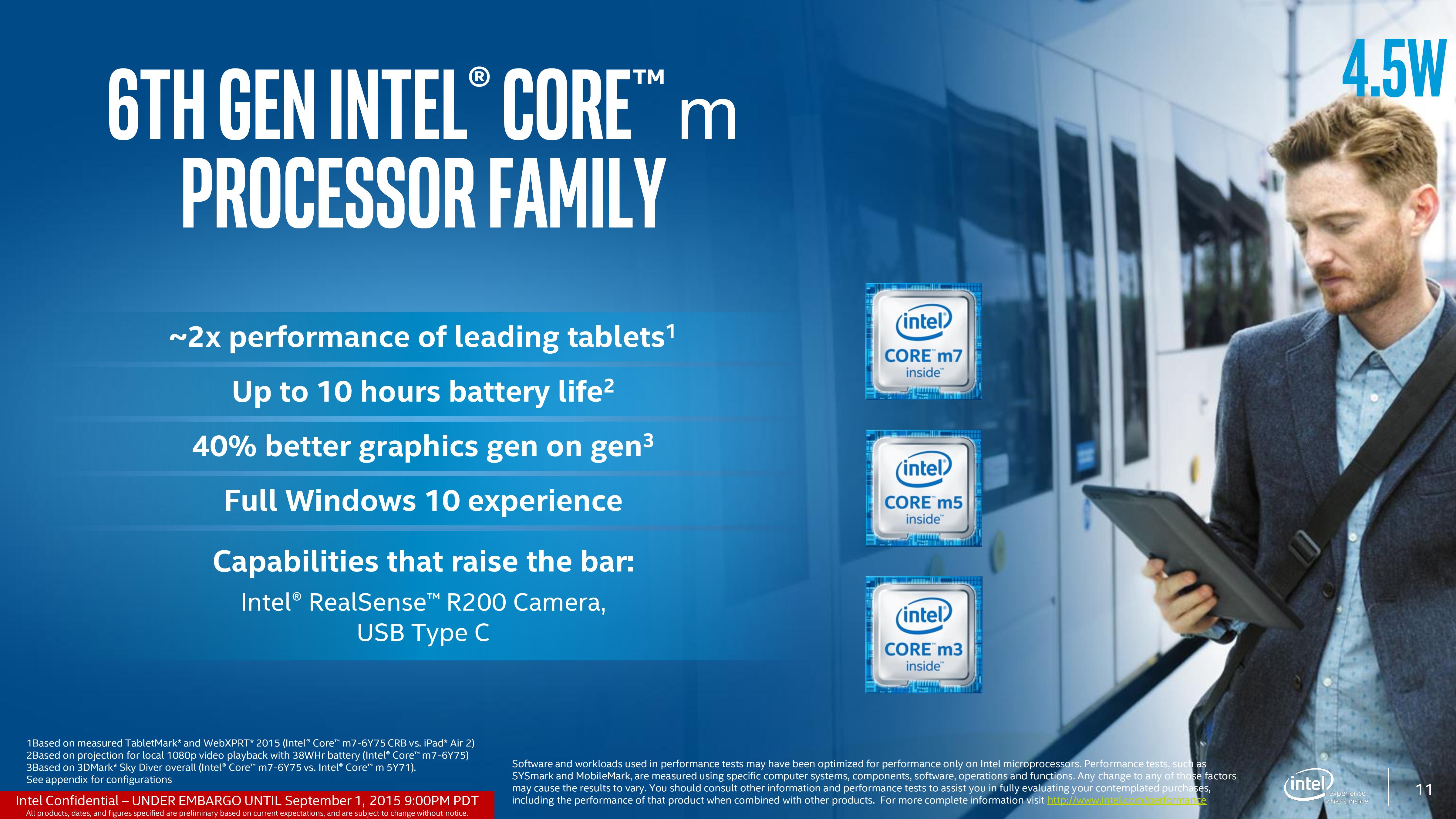
Starting at 4.5W, we spoke extensively with parts of Intel at IDF due to our Broadwell-Y coverage. From their perspective Broadwell-Y designs were almost too wide ranging, especially for what is Intel’s premium low-power high performance product, and for the vendors placing it in an ill-defined chassis far away from Intel’s recommended designs gave concern to the final performance and user experience. As a result, Intel’s guidelines to OEMs this generation are tightened so that the designers looking for the cheaper Core M plastic implementations can tune their design to get the best out of it. Intel has been working with a few of these (both entry Core M and premium models) to enact the user experience model.
Overall however, Intel is claiming 40% better graphics performance for Core M with the new Generation 9 (Gen9) implementation, along with battery saving and compatibility with new features such as RealSense. Because Core-M will find its way into products from tablets to 2-in-1s and clamshells, we’ve been told that the Skylake design should hit a home-run against the best-selling tablets in the market, along with an appropriate Windows 10 experience. When we get units in to review, we will see what the score is from our perspective on that one.
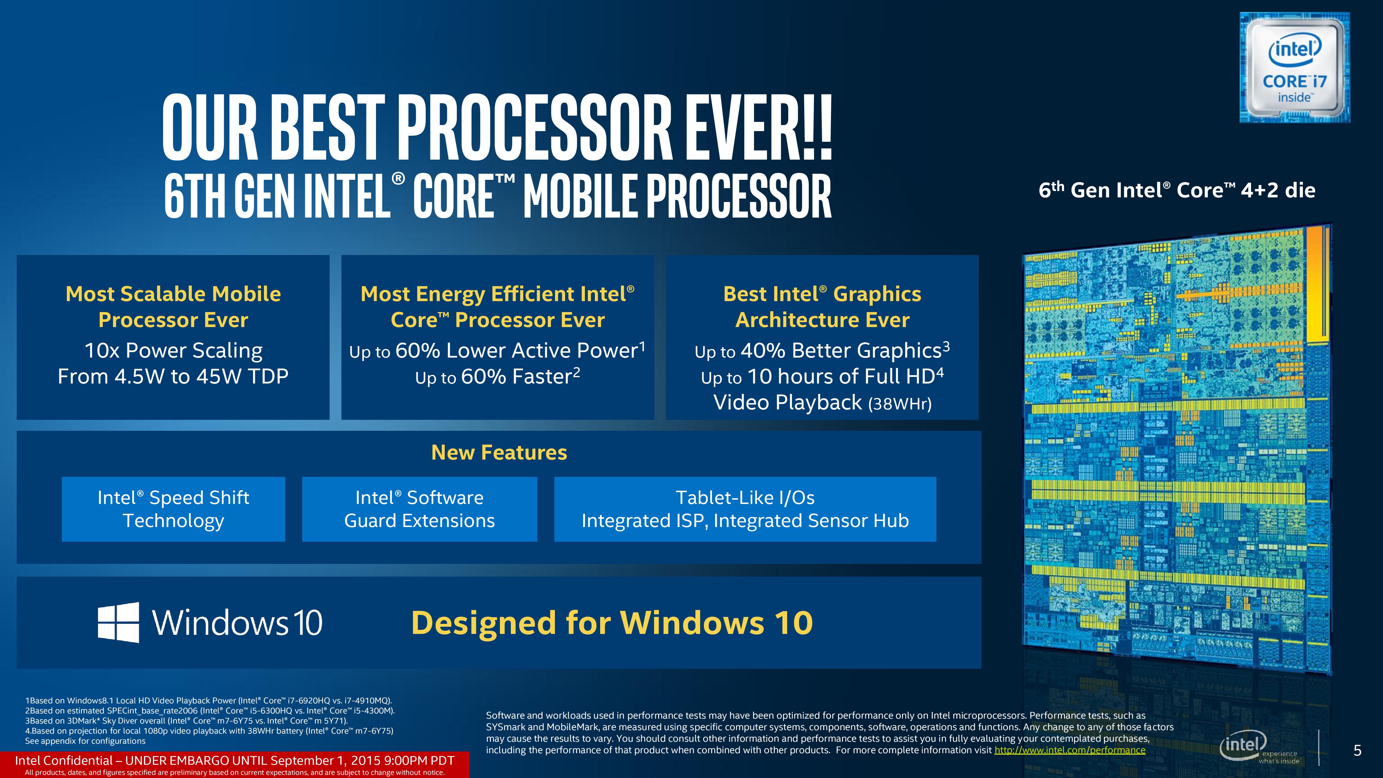
For the Skylake-Y to Skylake-U transition (and in part, Skylake-H), Intel is claiming a 60% gain in efficiency over Haswell-U. This means either 60% less active power during media consumption or 60% more CPU performance at the same power (measured by synthetics, specifically SPECint_base_rate2006). The power consumption metrics comes from updates relating to the Gen9 graphics, such as multi-plane overlay and fixed-function decoders, as well as additional power/frequency gating between the unslice and slices. We will cover this later in the review. The GPU itself, due to the new functionality, is claiming 40% better graphics performance for Core M during 3DMark synthetic tests.
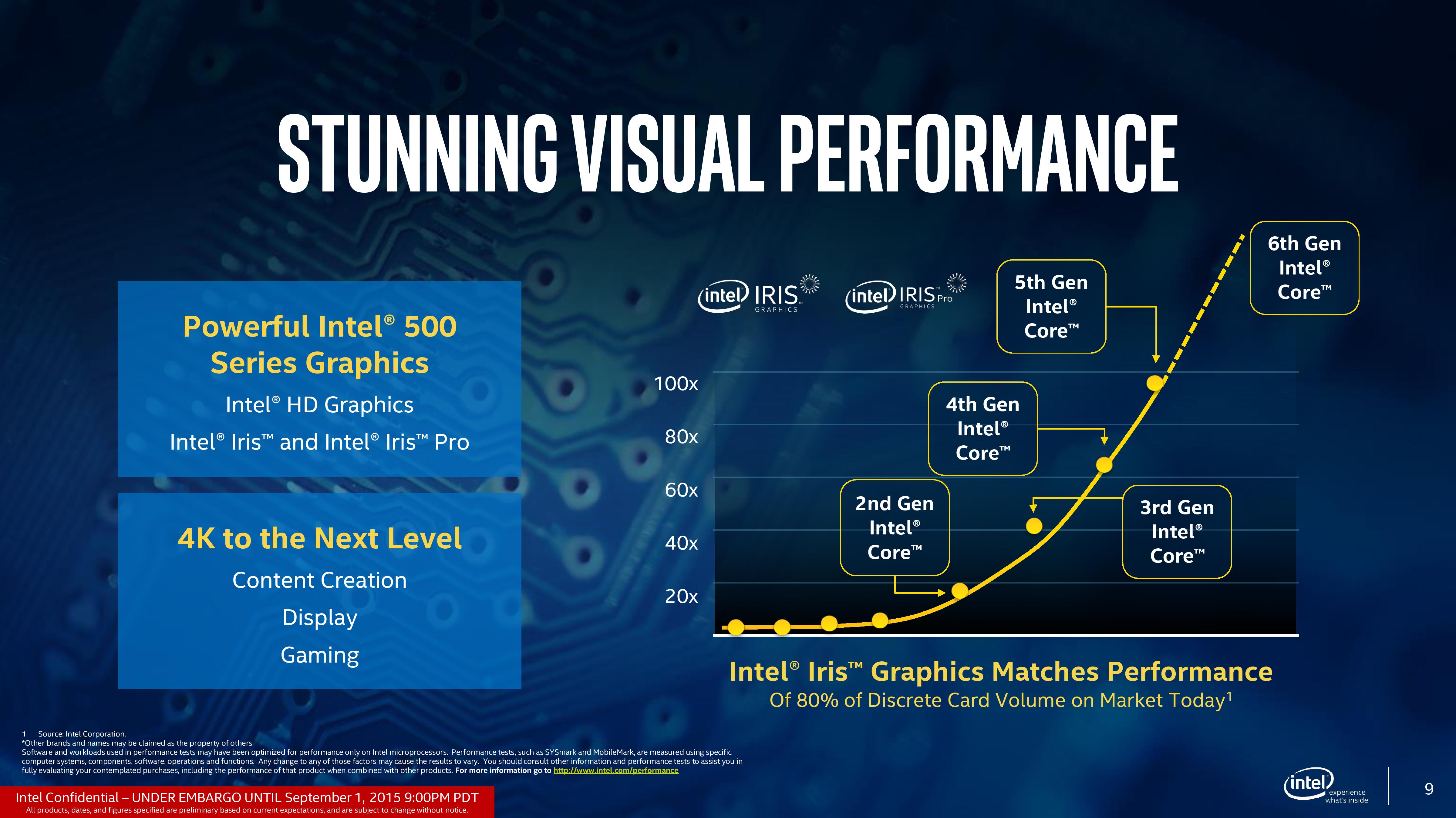
While not being launched today, Intel’s march on integrated graphics is also going to continue. With the previous eDRAM parts, Intel took the crown for absolute IGP performance from AMD, albeit being in a completely different price band. With Skylake, the introduction of a 4+4e model means that Intel’s modular graphics design will now extend from GT1 to GT4, where GT4e has 72 execution units with 128MB of eDRAM in tow. This leads to the claim that GT4e is set to match/beat a significant proportion of the graphics market today.
Back in our Skylake-K review, we were perhaps unimpressed with the generational gain in clock-for-clock performance, although improved multi-threading and frequency ranges helped push the out-of-the-box experience. The other side of that performance is the power draw, and because Skylake is another mobile-first processor, the power aspect becomes important down in mobile devices. We will go through some of these developments to improve power consumption in this article.


173 Comments
View All Comments
JKflipflop98 - Sunday, September 6, 2015 - link
Dude, if you're still running Arrandale, just about anything you buy at this point is going to be a *MAJOR* upgrade across the board.tipoo - Tuesday, September 1, 2015 - link
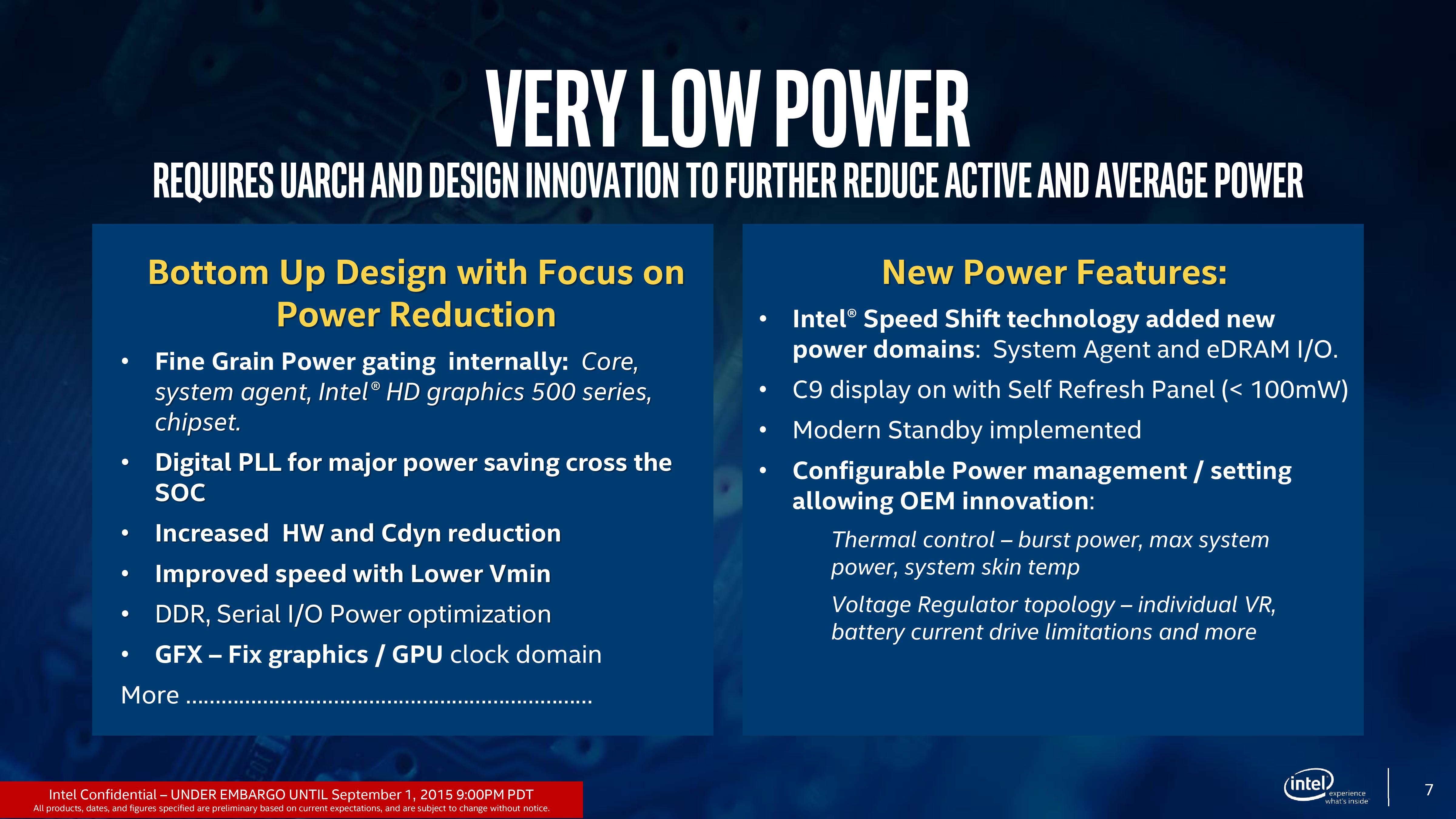
"Intel’s graphics topology consists of an ‘unslice’ (or slice common) that deals solely with command streaming, vertex fetching, tessellation, domain shading, geometry shaders, and a thread dispatcher. "This part of their architecture seemed like the weak spot which led to little scaling between 1/2/3 slices going from DX11 to DX12. So will that remain the same with Skylake, or are there other differences that will allow better scaling with DX12?
extide - Wednesday, September 2, 2015 - link
That sentence is actually incorrect (the quote).The unslice is not the same as slice common.
The Unslice is whats not in the slices, obviously, but the 'Slice Common' is what IS in the slice, but which ISNT the EU's themselves..
extide - Wednesday, September 2, 2015 - link
So, for example, GT2 has 1 Unslice, 3 Slice Commons (1/slice) and 24 EU's (8/slice).extide - Wednesday, September 2, 2015 - link
Actually it's GT2 has 1 Unslice, 1 Slice, 3 sub slices, 3 Slice Commons (1/subslice) and 24 EU's (8/subslice).ltcommanderdata - Tuesday, September 1, 2015 - link
Apple appears to take the Core M and use it in a 7 W cTDP up configuration in the Retina MacBook. I wonder if the increase in performance would be worth the increased heat and power consumption to use U-class processors in a 7.5 W cTDP down configuration instead? Or even try to accommodate 9.5 W cTDP down U-class processors to take advantage of the GT3e to better drive the retina display?Kutark - Tuesday, September 1, 2015 - link
I feel like i should know this already, but what are they referring to with the whole 4+2, 2+2 etc etc?Kutark - Tuesday, September 1, 2015 - link
Nm, i think i figured it out. 4core + GT2, or 2core +gt2, etc etcHideOut - Wednesday, September 2, 2015 - link
Yep, nailed it. (the +2/3/4 is GT2/3/4)Braincruser - Wednesday, September 2, 2015 - link
first number is CPU cores/modules, second part is gpu modules.