The Intel Skylake Mobile and Desktop Launch, with Architecture Analysis
by Ian Cutress on September 1, 2015 11:05 PM ESTIntel’s Generation 9 Graphics
On the graphics side of the equation, the information comes in two loaded barrels. For the media capabilities, including information regarding Multi Plane Overlay, Intel’s Quick Sync and HEVC decode, head on over to Ganesh’s great one page summary. Some of that information might be reproduced on this page to help explain some of the more esoteric aspects of the design.
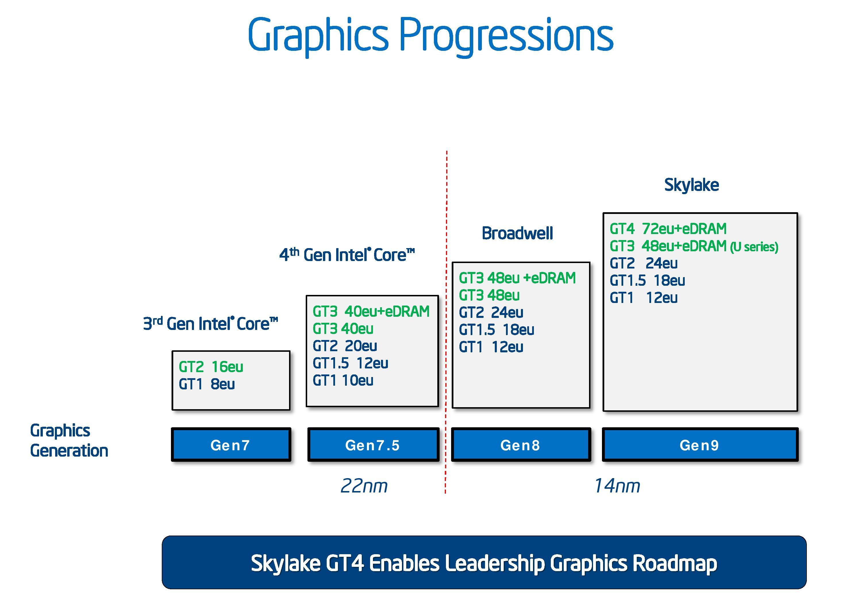
First let us look at how Intel’s integrated graphics has progressed over the generations. It has been no secret that the drive to integrated graphics has eaten almost all of the low end graphics market save one or two cards for extra monitor outputs. For Intel, this means slowly substituting a larger portion of the die to more execution units, as well as upgrading how those units process data. From the graphics above, and as we’ve noted before, Gen9 takes Gen8’s concept but with an added element at the top – GT4, which incorporates a new slice of EUs. As mentioned on the previous page, the eDRAM will come in 64 MB arrangements for GT3e (Iris), and 128 MB for GT4e (Iris Pro).
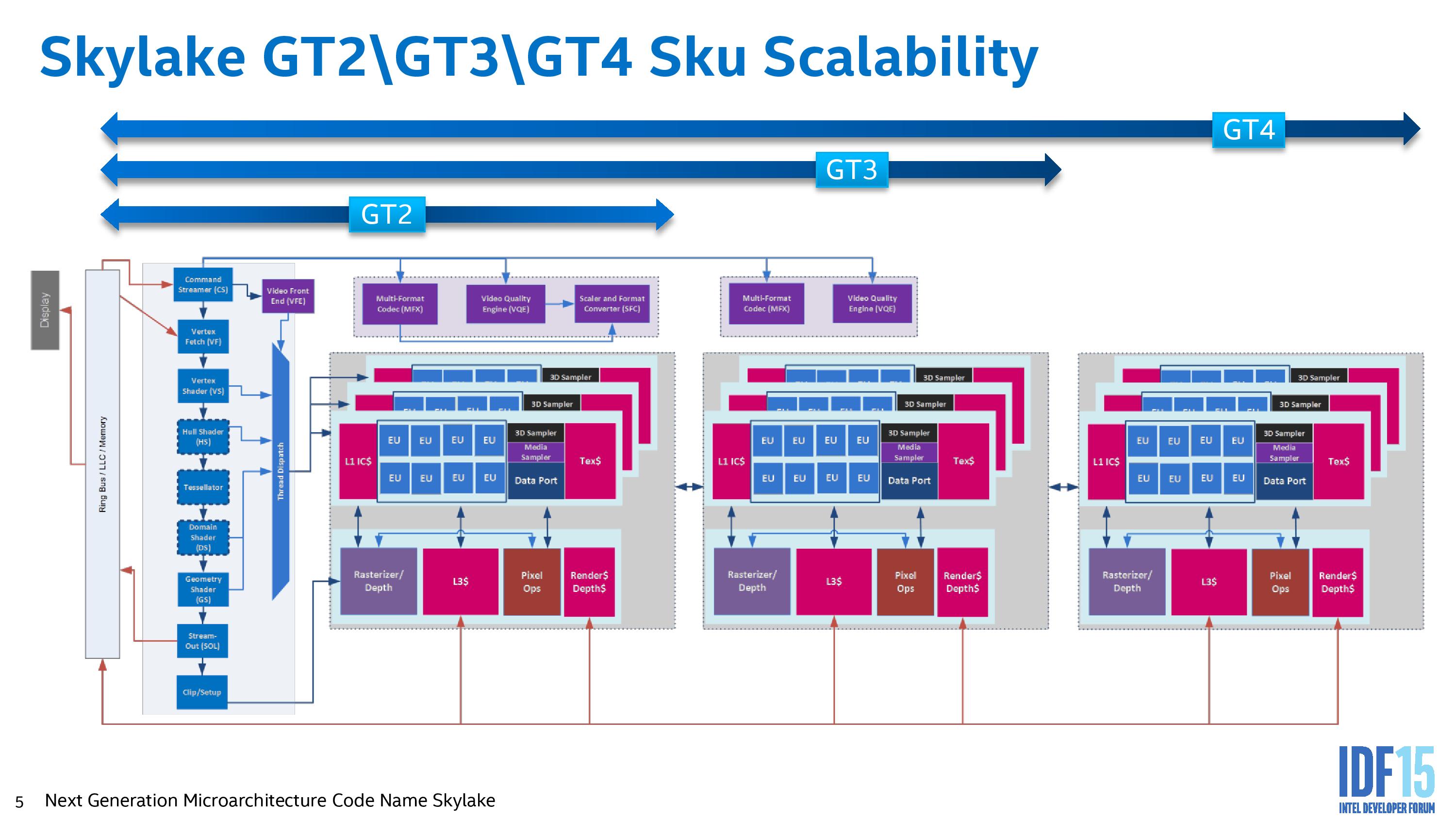
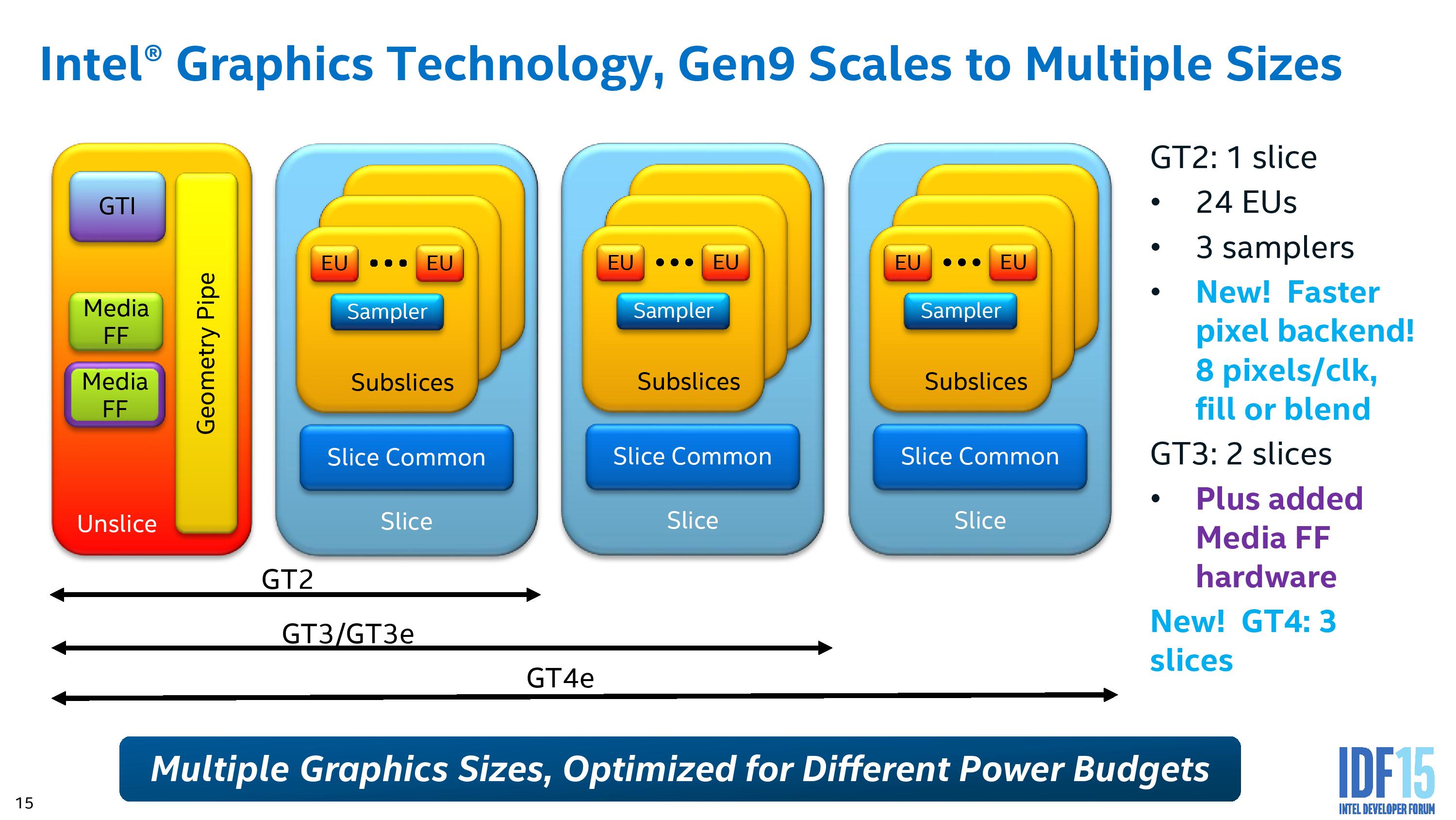
Intel’s graphics topology consists of an ‘unslice’ (or slice common) that deals solely with command streaming, vertex fetching, tessellation, domain shading, geometry shaders, and a thread dispatcher. This is followed up by either one, two or three slices, where each slice holds three sub-slices of 8 EUs, separate L1/L2/L3 caches and rasterizers, texture caches and media samplers. With one slice, a GT2 configuration of 24 EUs, we get the video quality engine (VQE), scalar and format converter (SFC) and a multi format codec engine (MFX). Moving to GT3 adds in another MFX and VQE.
| Intel Gen9 HD Graphics | |||||
| GPU Designation | Execution Units | GT | eDRAM? | YUHS | Example |
| Intel HD Graphics | 12 | 2+1 | - | Y | 4405Y |
| Intel HD Graphics 510 | 12 | 2+2 | - | U S | G4400 4405-U |
| Intel HD Graphics 515 | 24 | 2+2 | - | Y | 6Y75 6Y57 6Y30 |
| Intel HD Graphics 520 | 24 | 4+2 2+2 |
- | U | i7-6600U i3-6100U |
| Intel HD Graphics 530 | 24 | 4+2 2+2 |
- | H S | i7-6700K i3-6100T i7-6820HK |
| Intel HD Graphics P530 | 24 | 4+2 | - | H | E3-1535M v5 |
| Intel Iris Graphics 540 | 48 | 2+3e | 64MB | U | i7-6650U i5-6260U |
| Intel Iris Graphics 550 | 48 | 2+3e | 64MB | U | i7-6567U i3-6167U |
| Intel Iris Pro Graphics 580 | 72 | 4+4e | 128MB | H | - |


In each of the SKU lists, Intel has both the name of the graphics used as well as the base/turbo frequencies of the graphics. To synchronize both the name and the execution unit arrangement, we have the table above. At this point we have no confirmation of any parts having the GT1.5 arrangement, nor are we going to see any 23/24 EU combinations for Pentium/Celeron models similar to what we saw in Haswell. For the 12 EU arrangements, this means that these have a single slice of 24 EUs, but half of them are disabled. We questioned Intel on this back with Haswell, regarding of the EU cuts are split to 4/4/4 from the 8/8/8 sub-slice arrangement, and the answer we got back was interesting – there is no set pattern for 12 EU arrangements. It could be 4/4/4, or 3/4/5, or 3/3/6, or any other combination, as long as the performance is in line with what is expected and the EU count per sub-slice cannot be user probed. Despite the fact that a 3/3/6 arrangement might have L2 cache pressure in some circumstances, Intel feels that at this level of performance they can guarantee that the processors they ship will be consistent. It’s an interesting application.
Part of Intel’s strategy with the graphics is to separate all of these out as much as possible to different frequency planes and power gating, allowing parts of the silicon to only be powered when needed, or to offer more efficiency for regular use cases such as watching video.
The geometry pipe in the un-slice is improved to improve the triangle cull rate as well as remove redundant vertices, which aids an improved tessellated that creates geometry in a format (tri-stips) that can be resubmitted through the triangle cull when needed.

As we noted at Skylake-K launch, Gen 9 graphics also features lossless image compression allowing for fewer data transfers across the graphics subsystem. This saves both power and bandwidth, and an upgrade to the display controller allows the image format to be read in a compressed format so as not to uncompress it before it gets sent out to the display.
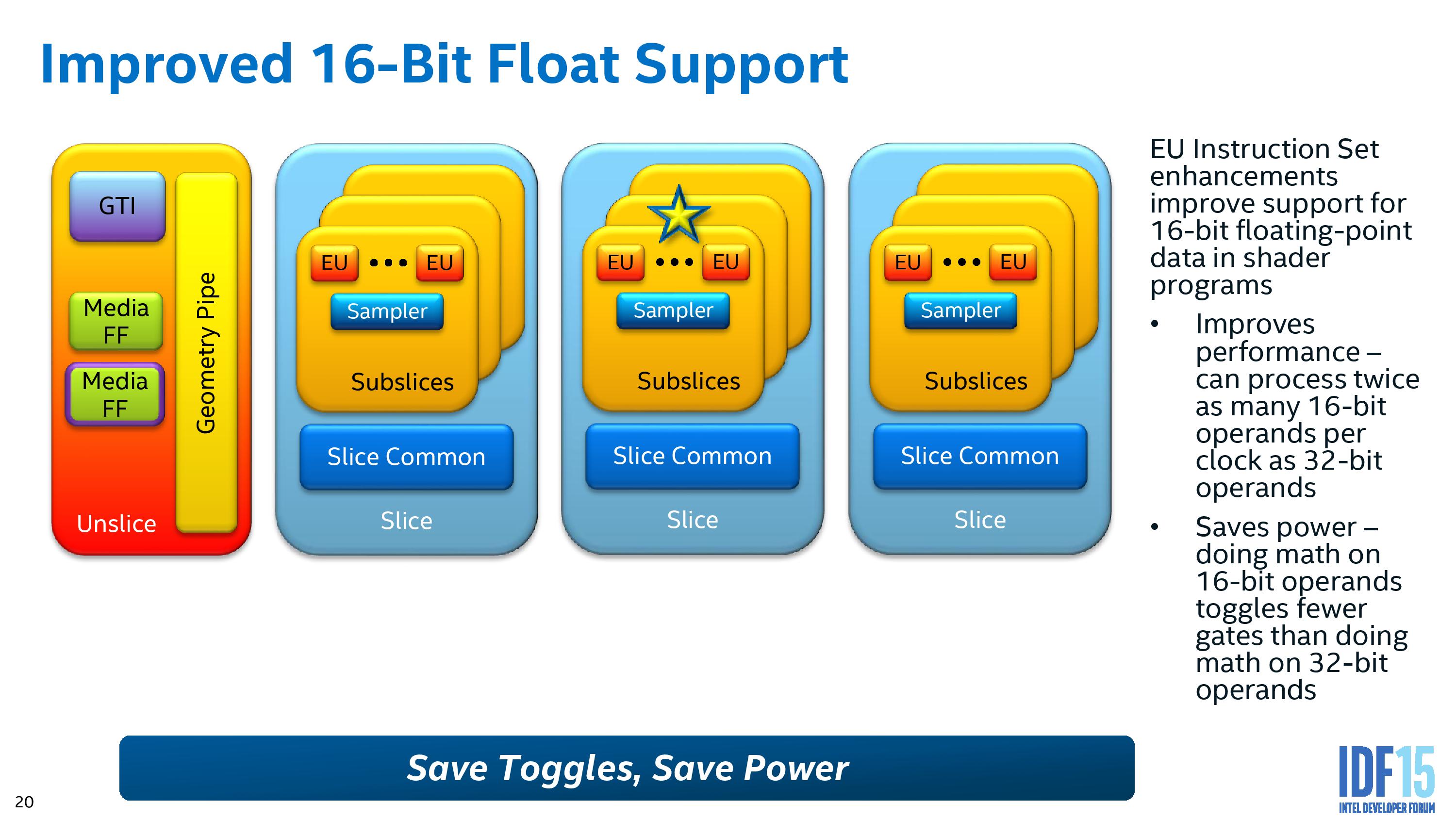
16-bit support has been a key element to discrete graphics in 2014 and 2015, affording faster processing when less accuracy is required by dumping extra significant digits. This is doubly beneficial, resulting in less power consumption for the same amount of work – Intel is exposing this to a greater degree in Gen9 for its shaders.
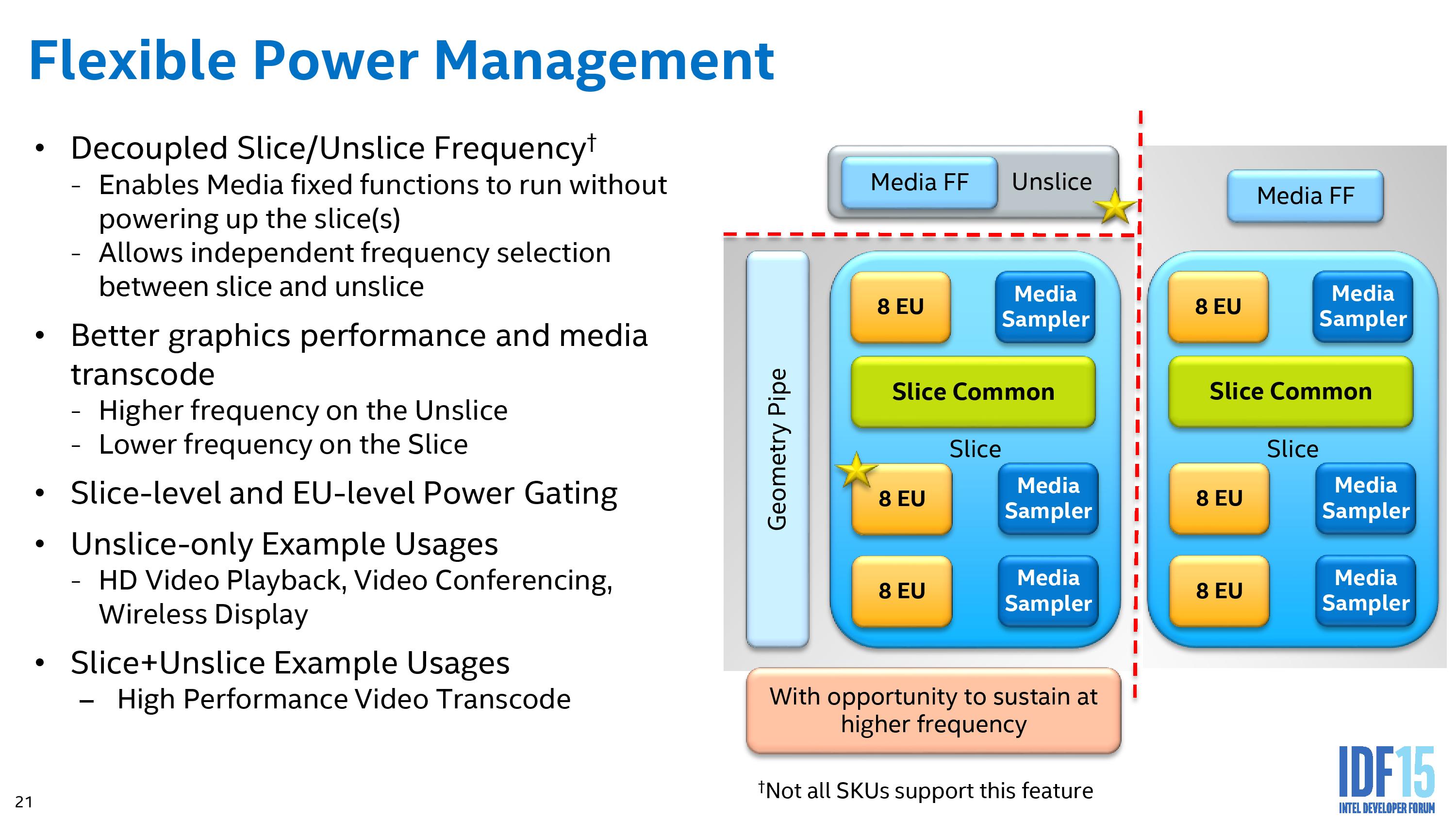
Intel’s big push on power for low-power Skylake is part of the reason why we did not see much difference in our Skylake-K review. Being able to shut off more parts of the processor that are not in use allows the available power budget to be applied to those that need it, hence why both power gating and frequency domains on the silicon, while they take up die area to implement, contribute to power saving overall or allow work to complete quicker in a race to sleep environment.
Multiplane Overlay (MPO)
One of the features I’m most particularly interested in is Multiplane Overlay. In a typical environment, a user might be looking at content that is stretched, rotated or distorted in some way. In order to perform this transformation, the image information is loaded into memory, siphoned off to the graphics to perform the mathematics, moved back into memory and then fired off to the display controller. This in and out of the DRAM costs power and battery life, so an attempt to mitigate this with fixed function hardware is ultimately beneficial. This is what MPO does.
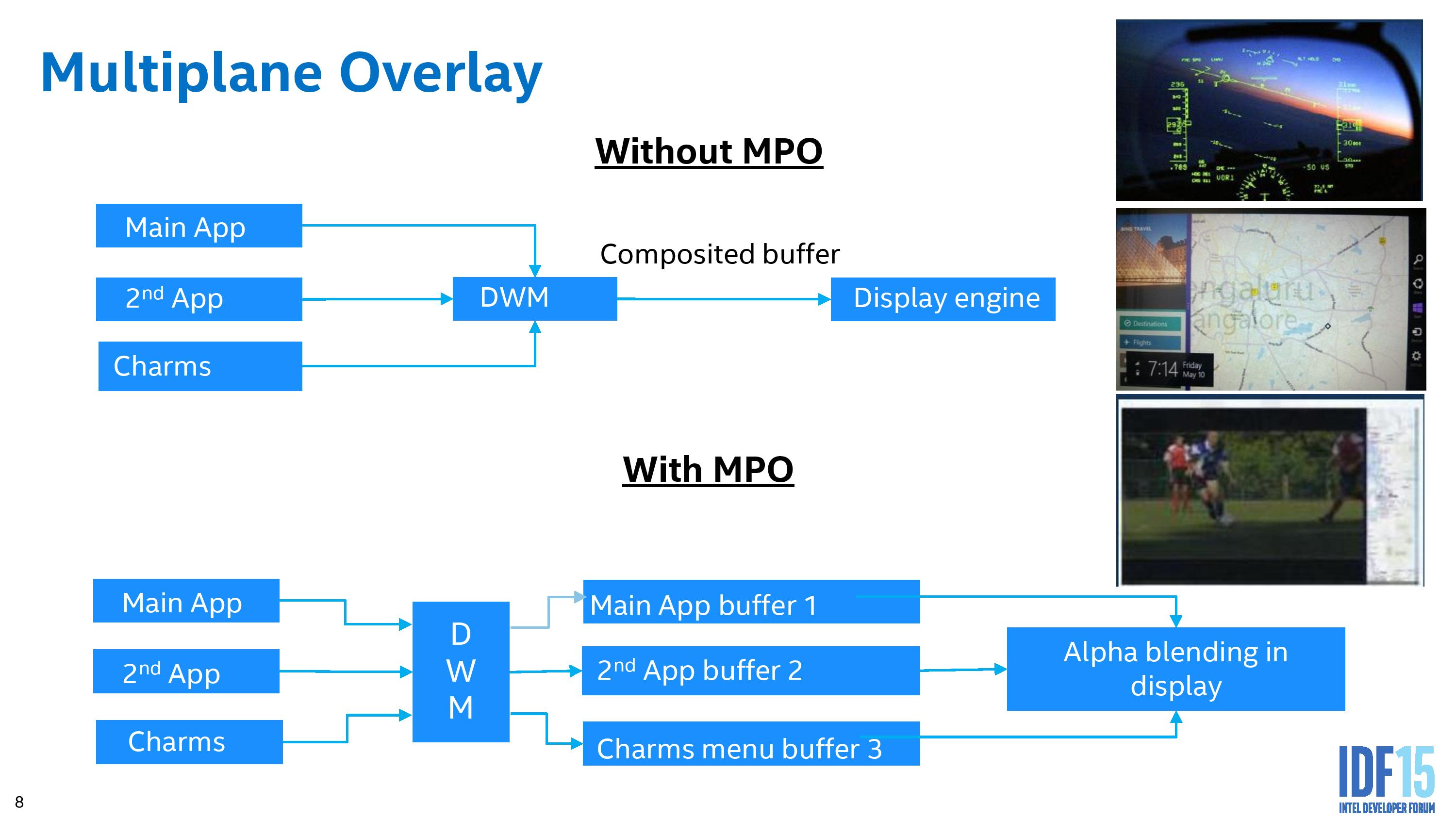
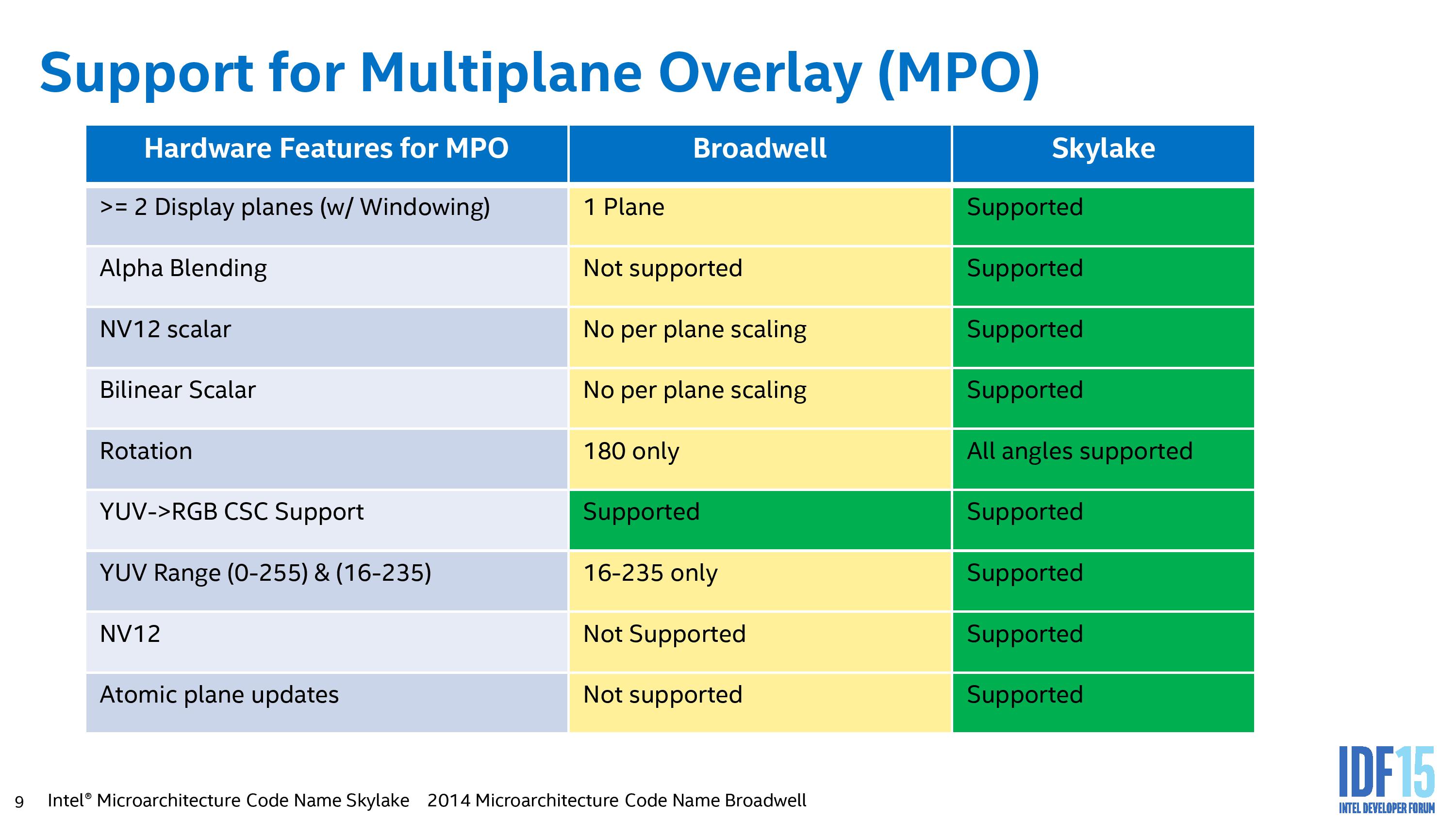
This slides shows a good way on how MPO works. The current implementation splits the screen into three ‘planes’ (app, background, cursor, or any combination therein) which are fired off to the desktop window manager (DWM). In a standard method, these layers are worked on separately before being composited and sent off to the display (the top model). With MPO, each of the planes fills a buffer in fixed function hardware on the display controller, without touching the GPU and requiring it to be put into a high power mode. MPO also allows for data in NV12 format to be processed on the fly as well, rather than requiring it all to be RGB before it is recombined into the final image (which again, saves power and bandwidth).
There are some limitations to this method. Currently, only three planes are supported, and there is no z-hierarchy meaning that if an app is obscured by another but still requires work, and then it does not get discarded as it should. For non-OS work that takes full-screen environments, it also requires the necessary hooks to the FF hardware otherwise it will assume it all as one plane and go back through the GPU. Intel is planning to improve this feature over time, as we might expect.
Intel’s data showed a 17% power saving increase overall while watching a 1080p24 video on a 1440p panel. Given the march to higher resolution displays and the lack of high resolution content, I can imagine this being an important player in future content consumption or multitasking.
There are a number of other media specific functions also new to Skylake, especially evolving around RAW processing in the fixed function units of the video quality engines to save power, other memory compression techniques and the encode/decode of specific formats such as HEVC and VP9. For this information, I suggest heading over to read Ganesh’s piece on Intel's Skylake GPU - Analyzing the Media Capabilities.


173 Comments
View All Comments
extide - Saturday, September 5, 2015 - link
Well, a decrease in performance from cannonlake to skylake would be correct. However, I assume you mean haswell, not cannonlake, and that is probably be due to the L2/FMUL changes. However you are also looking at chips with different clockspeeds, with haswell having a faster clock so that also contributes to this result.It is somewhat disappointing that Intel has decided to make changes that significantly favor power consumption over performance.
I have a feeling the Xeons will not have these same changes, so it will be interesting to see what the Skylake E5's are like...
shodanshok - Sunday, September 6, 2015 - link
Mmm, I have the very opposite feeling: I think that these changes were done explicitly to the benefit of server and mobile chips. These two categories (server and mobile) are greatly limited by their power usage (and by their ability to effectively remove the generated heart), while are only marginally dependent on FPU performance.So trading some performance for improved power efficiency suddenly make a lot of sense, especially if Intel want to continually increase Xeon's for number (and it seems so).
SeanJ76 - Saturday, September 5, 2015 - link
Not impressed...exmachiner - Monday, September 7, 2015 - link
Why is there no Desktop SKU with GT4e/Iris Pro ? Will it launch at a later date ? There is an Iris Pro version in Broadwell IIRC.ZachSaw - Monday, September 7, 2015 - link
I'd be interested to know what its relative performance is vs a discrete card like 750ti when it comes to the SM5.0 version of NNEDI3 with MPDN. Intel GPUs surprisingly run twice as fast with the shader version as compared to the OpenCL version (AMD loves shader too - the only exception here is NVIDIA's Maxwell architecture). It'll be interesting to see if Skylake is the perfect HTPC!janolsen - Tuesday, September 8, 2015 - link
If I understand pg 3 slide correctly , eDRAM will only be for BGA - and thus no Iris iGPU for desktop, broadwell chips may be a bit faster for those not needing a GPU for gaming and similar.HollyDOL - Wednesday, September 9, 2015 - link
Hm, is this a paper launch only? Only available parts until now are 6600K and 6700K (all czech big e-shops as well as ones like newegg). Awaiting 6100T eagerly (want to build mITX baby for my mom since her old (ancient) computer died 2 weeks ago)... and for obvious reasons I'd rather prefer new platform than the old one in case there was ever need to upgrade something (which I doubt but still...)qasdfdsaq - Thursday, September 10, 2015 - link
I feel like there's something missing here. We get 15w dual-core parts with Iris GT3e, but quad-core parts are all 45w with no GT3e. Indeed, there's no quad-core mobile chips with Iris graphics although Broadwell and Haswell both had them in the 45w quad-core range. There's certainly no issue fitting it in the power envelope, given you can literally fit 3x 2-core chips with GT3e into the 45w TDP.LDW - Friday, September 18, 2015 - link
I like to have a laptop for its portability and am not willing to buy a second system for my occasional gaming. In my experience, games like civ 5 , civ be and skyrim are happy with two processors but would like more graphics power than my current laptop. (i7-4700MQ with no additional graphics chips)...To my surprise, I find that the H series of processors have less graphics power than the U series. I suspect that the U series 2 processors, 4 threads would be just fine for the games I play and I know they would like the additional graphics power. So I'm likely to be looking at the U series as I look at replacements for my current laptop, not the H series as I expected.
I'm curious if others reach that conclusion as well.... and am looking forward to anandtech's future comparisons between the H and U series graphics capabilities.
ldw
francisca euralia - Tuesday, October 20, 2015 - link
hello, can u give me a sumary od this page with the most important definition?