The Intel Skylake Mobile and Desktop Launch, with Architecture Analysis
by Ian Cutress on September 1, 2015 11:05 PM ESTThe Claims
As with any launch, there are numbers abound from Intel to explain how the performance and experience of Skylake is better than previous designs as well as the competition.

As with Haswell and Broadwell, Intel is implementing a mobile first design with Skylake. As with any processor development structure the primal idea is to focus on one power point as being the most efficient and extend that efficiency window as far in either direction as possible. During IDF, Intel stated that having an efficiency window from 4.5W to 91W is a significant challenge, to which we agree, as well as improving both performance and power consumption over Broadwell at each stage.
Starting at 4.5W, we spoke extensively with parts of Intel at IDF due to our Broadwell-Y coverage. From their perspective Broadwell-Y designs were almost too wide ranging, especially for what is Intel’s premium low-power high performance product, and for the vendors placing it in an ill-defined chassis far away from Intel’s recommended designs gave concern to the final performance and user experience. As a result, Intel’s guidelines to OEMs this generation are tightened so that the designers looking for the cheaper Core M plastic implementations can tune their design to get the best out of it. Intel has been working with a few of these (both entry Core M and premium models) to enact the user experience model.
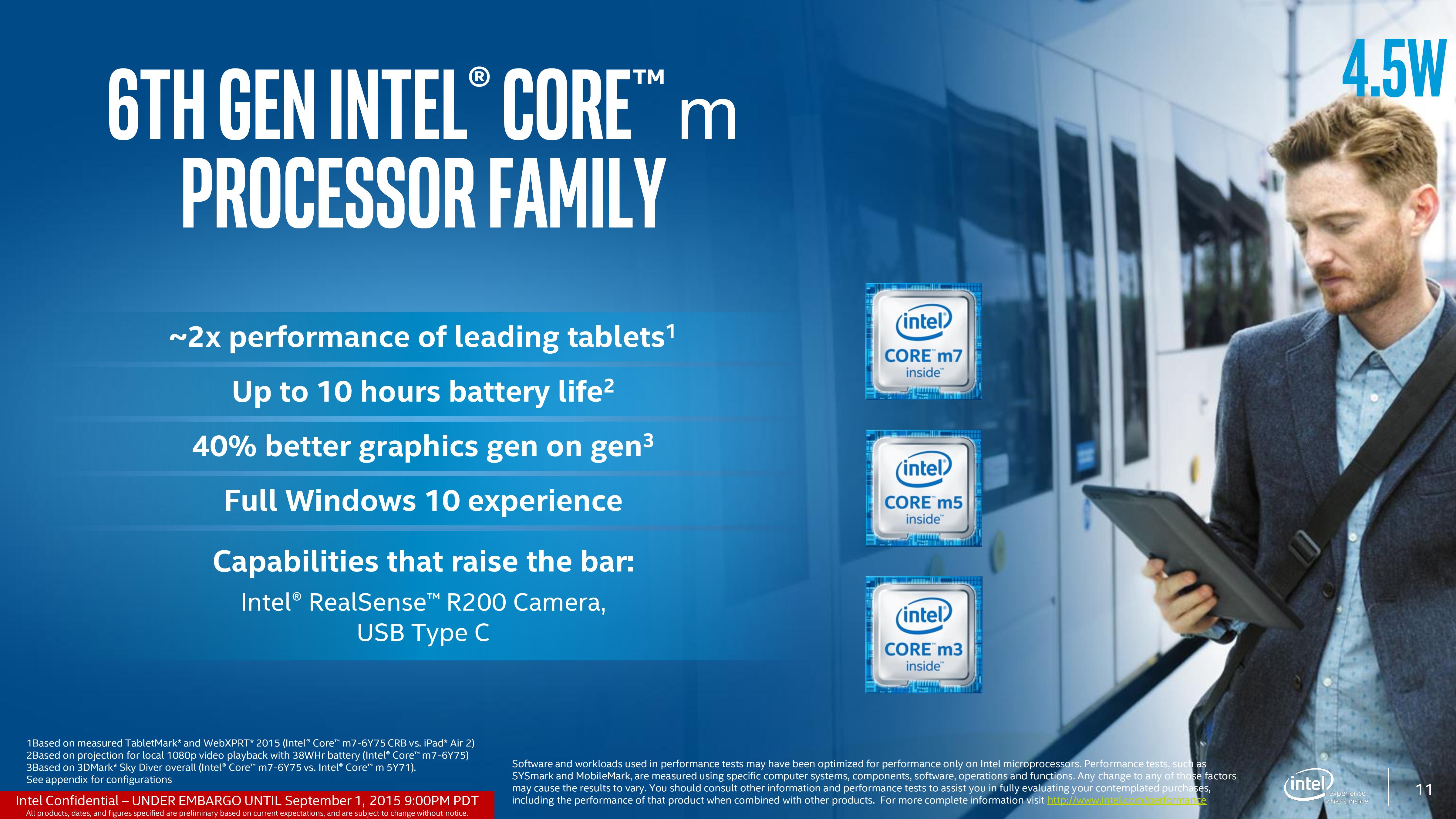
Overall however, Intel is claiming 40% better graphics performance for Core M with the new Generation 9 (Gen9) implementation, along with battery saving and compatibility with new features such as RealSense. Because Core-M will find its way into products from tablets to 2-in-1s and clamshells, we’ve been told that the Skylake design should hit a home-run against the best-selling tablets in the market, along with an appropriate Windows 10 experience. When we get units in to review, we will see what the score is from our perspective on that one.
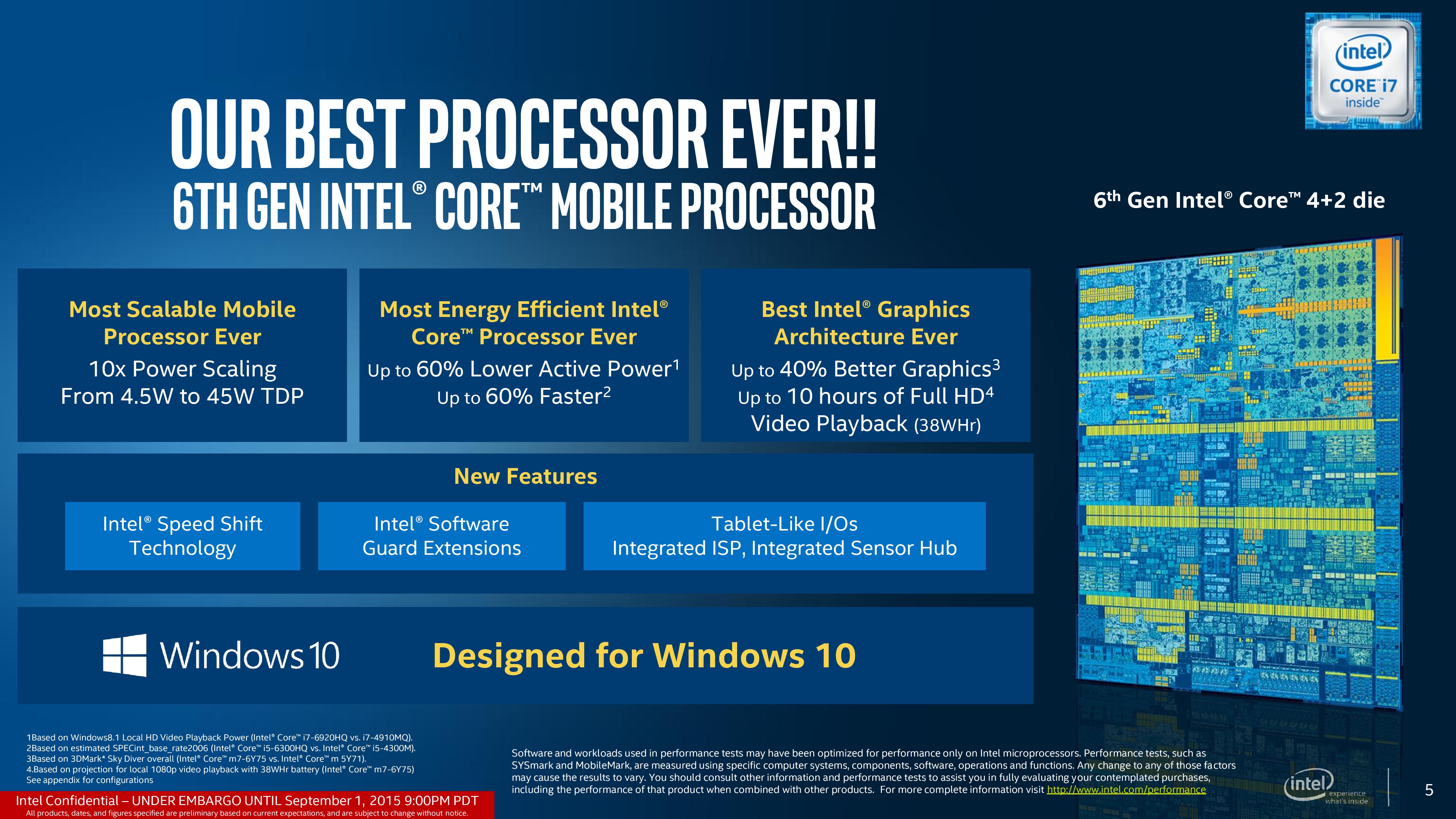
For the Skylake-Y to Skylake-U transition (and in part, Skylake-H), Intel is claiming a 60% gain in efficiency over Haswell-U. This means either 60% less active power during media consumption or 60% more CPU performance at the same power (measured by synthetics, specifically SPECint_base_rate2006). The power consumption metrics comes from updates relating to the Gen9 graphics, such as multi-plane overlay and fixed-function decoders, as well as additional power/frequency gating between the unslice and slices. We will cover this later in the review. The GPU itself, due to the new functionality, is claiming 40% better graphics performance for Core M during 3DMark synthetic tests.
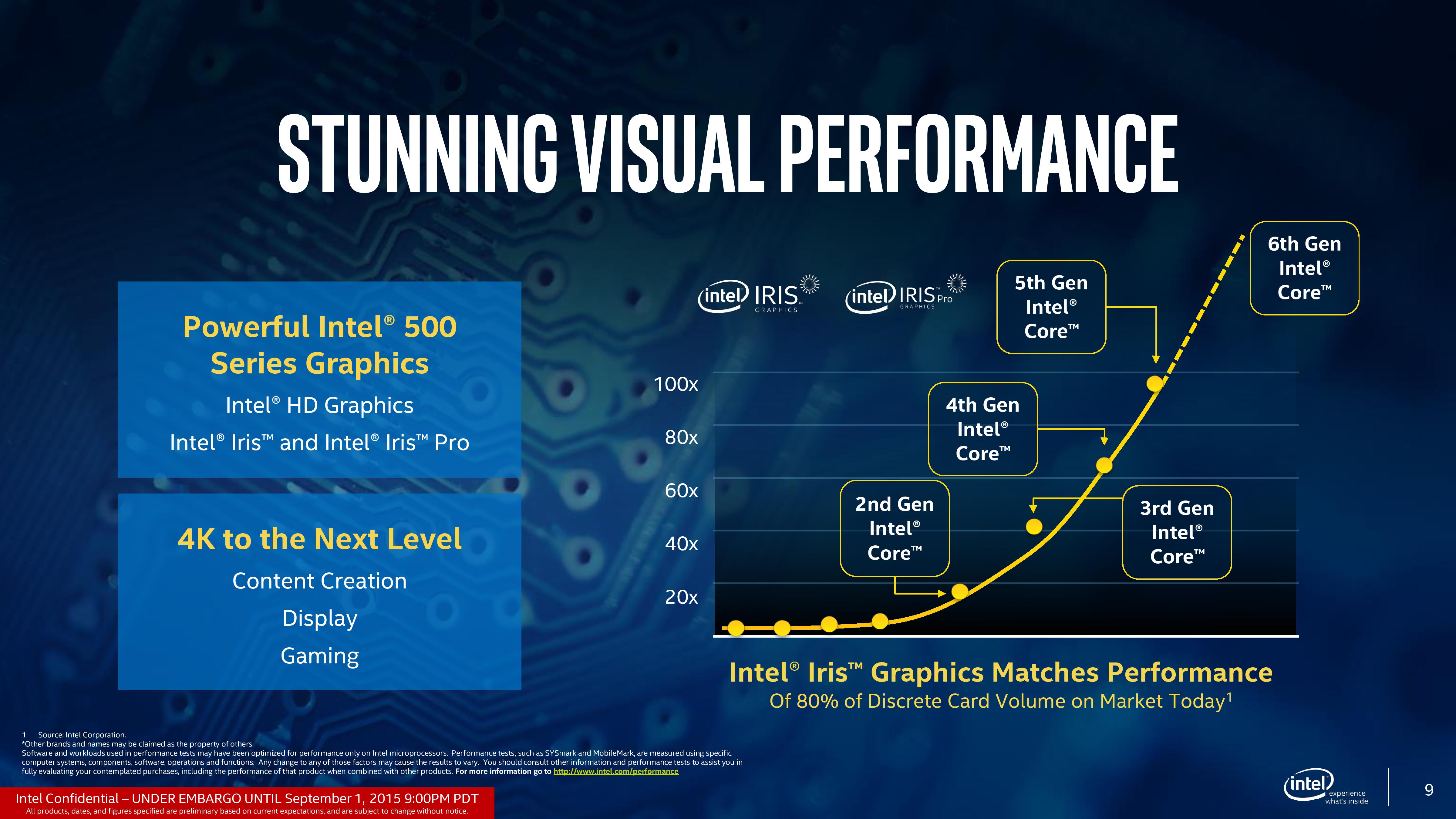
While not being launched today, Intel’s march on integrated graphics is also going to continue. With the previous eDRAM parts, Intel took the crown for absolute IGP performance from AMD, albeit being in a completely different price band. With Skylake, the introduction of a 4+4e model means that Intel’s modular graphics design will now extend from GT1 to GT4, where GT4e has 72 execution units with 128MB of eDRAM in tow. This leads to the claim that GT4e is set to match/beat a significant proportion of the graphics market today.
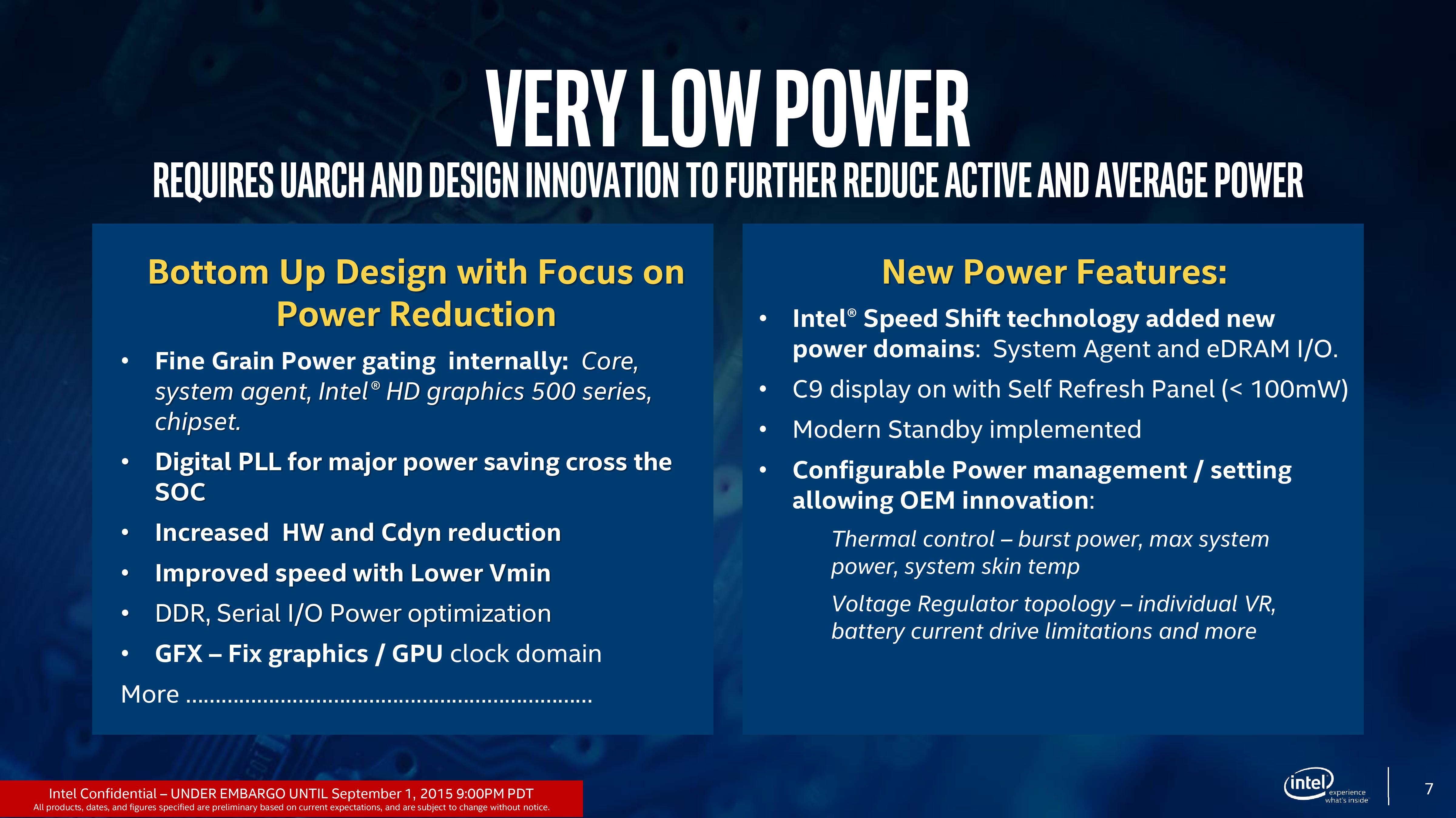
Back in our Skylake-K review, we were perhaps unimpressed with the generational gain in clock-for-clock performance, although improved multi-threading and frequency ranges helped push the out-of-the-box experience. The other side of that performance is the power draw, and because Skylake is another mobile-first processor, the power aspect becomes important down in mobile devices. We will go through some of these developments to improve power consumption in this article.


173 Comments
View All Comments
prisonerX - Thursday, September 3, 2015 - link
You can't make a purse out of a sow's ear.BMNify - Saturday, September 5, 2015 - link
"prisonerX - Thursday, September 03, 2015You can't make a purse out of a sow's ear."
hmm
https://libraries.mit.edu/archives/exhibits/purse/...
Report: "On the Making of Silk Purses from Sows' Ears," 1921
https://libraries.mit.edu/archives/exhibits/purse/...
extide - Saturday, September 5, 2015 - link
Yeah that's because they are starting with a MUCH MUCH less refined architecture. It's easy to improve a ton on something that isnt as good to begin with... Plus, there is only so much you can do, you quickly run into diminishing returns.This is seriously like one of the simplest concepts ever but people still don't seem to get it....
BMNify - Saturday, September 5, 2015 - link
"extide: Plus, there is only so much you can do, you quickly run into diminishing returns."that's a subjective POV, if you where to remove the base sram and dram and replace them with 10s of femto seconds Correlated Electron RAM and/or Mram in both sram and new wideIO2 configurations for these Arm invested NVram and role them out in the usual arm/foundry collaborations then you begin to see the latest advertised Intel far slower new "3D XPoint" as a sub standard technology in comparison ....
http://www.zdnet.com/article/arm-licenses-next-gen...
Galatian - Thursday, September 3, 2015 - link
"For users who actively want an LGA1151 4+4e configuration, make sure your Intel representative knows it, because customer requests travel up the chain."Who do I need to talk to? Seriously I didn't get Broadwell because I knew Skylake was right around the corner. I mean why introduce a pocketable 5x5 platform, just to announce that you have no plans to actually release the perfect processor for that platform?
Valantar - Thursday, September 3, 2015 - link
"For Skylake-U/Y, these processors are not typically paired with discrete graphics and as far as we can tell, the PCIe lanes have been removed from these lines. As a result, any storage based on PCIe (such as M.2) for devices based on these processors will be using the chipset PCIe lanes."According to Intel Ark, the 15W U-series CPUs (at least the i5s and i7s (including the Iris 6650U), which I looked at) have 12 PCIe 3.0 lanes, available in "1x4, 2x2, 1x2+2x1 and 4x1" configurations. Worth updating the article?
Valantar - Thursday, September 3, 2015 - link
And reading on, I suddenly realize why you said what you did. 12 lanes does indeed line up with the ones from the PCH-LP. Does this point toward more of an SOC-like integration of features for U-/Y-series CPUs?BMNify - Thursday, September 3, 2015 - link
"A lot of these improvements are aimed directly at the pure-performance perspective (except L2 and FMUL to an extent), so you really have to be gunning it or have a specific workload to take advantage."i cant believe that to be true, as its a tock and yet no real world view can call this tock an improvement never mind "so you really have to be gunning it or have a specific workload to take advantage." as the real world x264/x265 show no benefit what so ever here....
also Ian, was it an oversight on your part that in all the 9 pages analysis you did not point out the missing generic "AVX2 SIMD" in most of all these launched today.... please note that the official Intel slides pacifically remove any mention of any AVX SIMD in their latest charts etc.
it seems a clear cut choice on intels part to try and stop news outlets from mentioning and pointing out the lack of 2015 class SIMD on many of these soc released today.....
can you at least go through the included charts and point out all the cores/soc that Do Not include generic AVX2 SIMD to make it clear which cores/soc to actually buy (anything with AVX2+) and what new/old soc to discard (anything with only antiquated 2006 sse4 SIMD)
Xenonite - Thursday, September 3, 2015 - link
Actually, consumers will actively avoid AVX2 instruction set capable processors, since they could use more power (especially on the desktop, where Intel's power limiter allows AVX2 to really boost application performance / power consumption)BMNify - Monday, September 7, 2015 - link
i dont see any logic to your "consumers will actively avoid AVX2 instruction set " comment as by definition "SIMD" ( Single Instruction, Multiple Data) describes computers with multiple processing elements that perform the same operation on multiple data points simultaneously.so in fact AVX2 256 bit SIMD does exactly the opposite of wasting more power compared to the older/slower data paths today, also its clear in the mobile/ultra low power devices where "Qualcomm's new DSP technology boasts heavy vector engine—that it calls Hexagon Vector eXtensions or HVX—for compute-intensive workloads in computational photography, computer vision, virtual reality and photo-realistic graphics on mobile devices. Moreover, it expands single instruction multiple data (SIMD) from 64-bit to 1,024-bit in order to carry out image processing with a wider vector capability...." is in fact doubling even intel's as yet unreleased 512bit AVX3 , with their lowest power 1,024-bit SIMD to date, although its unknown weather its a refreshed NEON or another complimentary SIMD there... we shall see soon enough.