The IBM POWER8 Review: Challenging the Intel Xeon
by Johan De Gelas on November 6, 2015 8:00 AM EST- Posted in
- IT Computing
- CPUs
- Enterprise
- Enterprise CPUs
- IBM
- POWER
- POWER8
The L4-cache and Memory Subsystem
Each POWER8 memory controller has access to four "Custom DIMMs" or CDIMMs. Each CDIMMs is in fact a "Centaur" chip and 40 to 80 DRAM chips. The Centaur chip contains the DDR3 interfaces, the memory management logic and a 16 MB L4-cache.
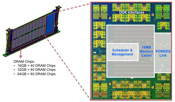
The 16 MB L4-cache is eDRAM technology like the on-die L3-cache. Let us see how the CDIMMs look in reality.
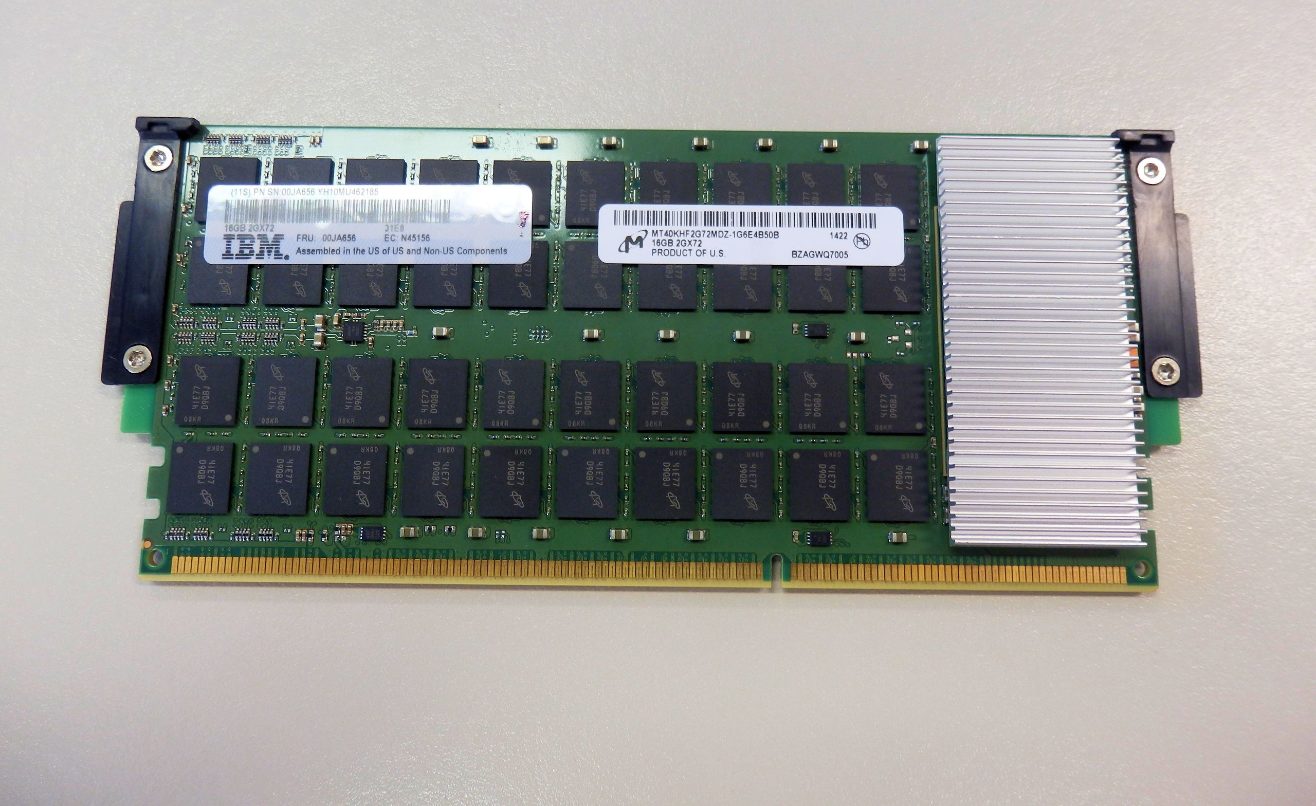
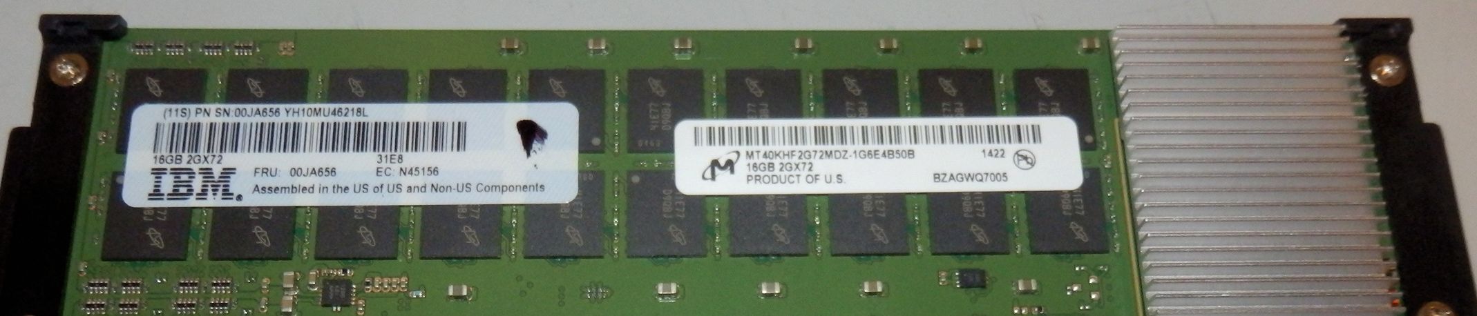
Considering that 4Gb DRAM chips were available in mid 2013, the 1600 MHz 2Gb DRAM chips used here look a bit outdated. Otherwise the (much) more expensive 64GB CDIMMs use the current 4Gb DRAM chips. The S822L has 16 slots and can thus use up to 1TB (64GB x 16) in DIMMs.
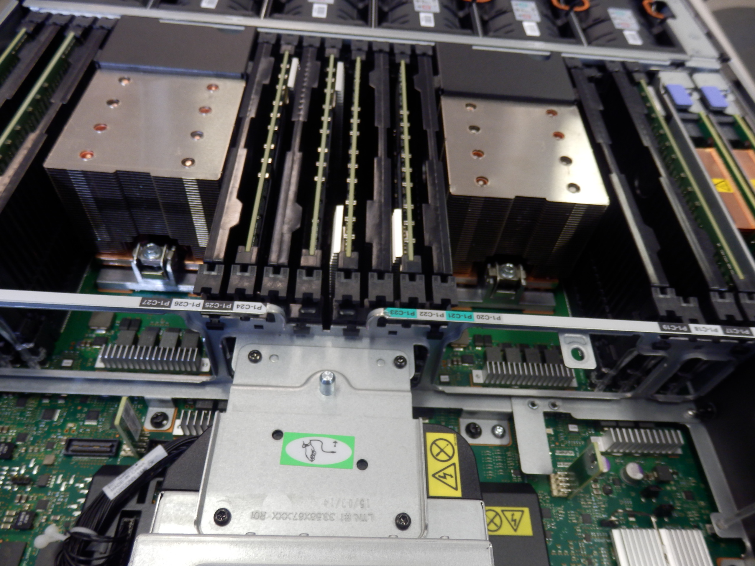
Considering that many Xeon E5 servers are limited to 768 GB, 1 TB is more than competitive. Some Xeon E5 servers can reach 1.5 TB with 64 GB LR-DIMMs but not every server supports this rather expensive memory technology. It is very easy to service the CDIMMs: a gentle push on the two sides will allow you to slide them out. The black pieces of plastic between the CDIMMS are just place-holders that protect the underlying memory slots. For our testing we had CDIMMs installed in 8 of our system's 16 slots.
The Centaur chip acts as a 16MB L4-cache to save memory accesses and thus energy, but it needs quite a bit of power (10-20 W) itself and as a result is covered by heatsink. CDIMMs have ECC enabled (8+1 for ECC) and have also an extra spare DRAM chip. As result, a CDIMM has 10 DRAM chips while offering capacity of 8 chips.
That makes the DRAM subsystem of the S822L much more similar to the E7 memory subsystem with the "Scalable memory interconnect" and "Jordan Creek" memory buffer technology than to the typical Xeon E5 servers.


146 Comments
View All Comments
FunBunny2 - Friday, November 6, 2015 - link
"The z10 processor was co-developed with and shares many design traits with the POWER6 processor, such as fabrication technology, logic design, execution unit, floating-point units, bus technology (GX bus) and pipeline design style, i.e., a high frequency, low latency, deep (14 stages in the z10), in-order pipeline." from the Wiki.Yes, the z continues the CISC ISA from the 360 (well, sort of) rather than hardware RISC, but as Intel (amongst others) has demonstrated, CISC ISA doesn't have to be in hardware. In fact, the 360/30 (lowest tier) was wholly emulated, as was admitted then. Today, we'd say "micro-instructions". All those billions of transistors could have been used to implement X86 in hardware, but Intel went with emulation, sorry micro-ops.
What matters is the underlying fab tech. That's not going anywhere.
FunBunny2 - Friday, November 6, 2015 - link
^^ should have gone to KevinG!!Kevin G - Saturday, November 7, 2015 - link
The GX bus in the mainframes was indeed shared by POWER chips as that enabled system level component sharing (think chipsets).However, attributes like the execution unit and the pipeline depth are different between the POWER6 and z10. At a bird's eye view, they do look similar but the implementation is genuinely different.
Other features like SMT were introduced with the POWER5 but only the most recent z13 chip has 2 way SMT. Features like out-of-order execution, SMT, SIMD were once considered too exotic to validate in the mainframe market that needed absolute certainty in its hardware states. However, recent zArch chips have implemented these features, sometimes decades after being introduced in POWER.
The other thing is that IBM has been attempting to get get more and more of the zArch instruction set to be executed by hardware and no microcode. Roughly 75% to 80% of instructions are handled by microcode (there is a bit of a range here as some are conditional to use microcode).
JohanAnandtech - Saturday, November 7, 2015 - link
I believe that benchmark uses about 8 threads and not very well either? Secondly, it is probably very well optimized for SSE/AVX. So you can imagine that the POWER8 will not be very good at it, unless we manually optimize it for Altivec/VSX. And that is beyond my skills :-)UrQuan3 - Monday, December 21, 2015 - link
I'm sure no one is still reading this as I'm posting over a month later, but...I tested handbrake/x264 on a bunch of cross-platform builds including Raspberry Pi 2. I found it would take 24 RPi2s to match a single i5-4670K. That was a gcc compiled handbrake on Raspbian vs the heavily optimized DL copy for Windows. Not too bad really. Also, x264 seems to scale fairly well with the number of cores. Still, POWER8 unoptimized would be interesting, though not a fair test.
BTW, I'd encourage you to use a more standard Linux version than 6-month experimental little-endian version of Ubuntu. The slides you show advertise support for Ubuntu 14.04 LTS, not 15.04. For something this new, you may need the latest, but that is often not the case.
stun - Friday, November 6, 2015 - link
@Johan You might want to fix "the platform" hyperlink at the bottom of page 4. It is invalid.JohanAnandtech - Friday, November 6, 2015 - link
Thanks and fixed.Ahkorishaan - Friday, November 6, 2015 - link
Couldn't read past the graphic on page 1. It's 2015 IBM, time to use a font that doesn't look like a toddler's handwriting.xype - Sunday, November 8, 2015 - link
To be fair, it seems that the slide is meant for management types… :PJtaylor1986 - Friday, November 6, 2015 - link
Using decimals instead of commas to denote thousands is jarring to your North American readers.