Analyzing Intel-Micron 3D XPoint: The Next Generation Non-Volatile Memory
by Kristian Vättö, Ian Cutress & Ryan Smith on July 31, 2015 11:00 AM ESTEstimating 3D XPoint Die Size
By now most of you probably know that I'm a sucker for die sizes and since this is information that the DRAM and NAND vendors are unwilling to share, I've gone as far as developing my own method for estimating the die size (well, it's really just primary school geometry, so I can't take too much credit for it). Die size is the key factor in determining cost efficiency because it directly relates to the number of gigabytes each wafer yields and thus it's a vital metric for comparing different technologies and process nodes.
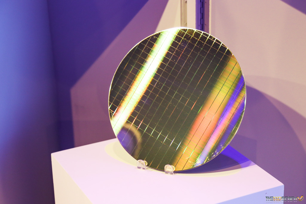
I'm borrowing the above picture from The SSD Review because to be honest my wafer photos (and photos in general) are quite horrible and wafers are far from being the easiest object given all the reflections. Sean is a professional photographer, so he managed to grab this clear and beautiful photo of the production 3D XPoint wafer Intel and Micron had on display, making it easy to estimate the die size.
I calculated 18 dies horizontally and 22 vertically, which yields 227mm^2 with a normal 300mm wafer. When taking die cuts (i.e. the space between dies) into account, we should be looking at 210-220mm^2. Array efficiency is about 90%, which is much higher than planar NAND because most of the peripheral circuitry lies underneath the memory array.
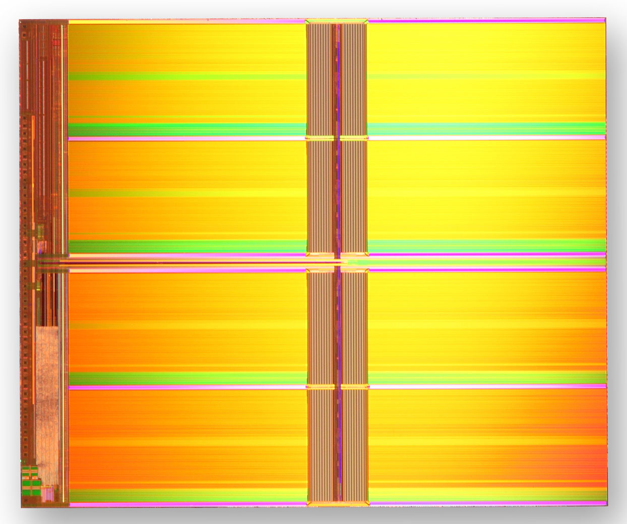
IMFT 20nm 128Gbit MLC NAND die
For comparison, Intel-Micron's 20nm 128Gbit MLC NAND die measures 202mm^2 and has array efficiency of ~75%. From that we can calculate that the 128Gbit memory array in 3D XPoint takes about 190mm^2, while a similar capacity planar NAND array measures ~150mm^2 (since the 128Gbit 3D XPoint die consists of two layers and 128Gbit MLC NAND die stores two bits per cell, the number of layers and bits stored per cell cancel out). It seems like NAND is denser (about 20-25%) from a memory array perspective given a fixed feature size (i.e. lithography), but at this point it's hard to say whether this is due to the cell design itself or something else. Connecting layers of wordlines and bitlines to the intermetal layers likely takes some extra area compared to a 2D process (at least this is the case with 3D NAND), which might partially explain the lower density compared to NAND.
However we will have to wait for some SEM photos to really see what's happening inside the 3D XPoint array and how it compares to NAND in cell size and overall density efficiency. Of course, there is a lot more in total manufacturing cost than just the cell and die size, but I'll leave the full analysis to those with the proper equipment and deeper knowledge of semiconductor manufacturing processes.
What Happens to 3D NAND
The above analysis already gives a hint that 3D XPoint isn't about to replace 3D NAND, at least not in the foreseeable future. That's also what Intel and Micron clearly stated when asked about 3D XPoint's impact on 3D NAND because it's really a new class of memory that fills a niche that DRAM and NAND cannot. The companies are still looking forward to rolling out 3D NAND next year and have a strong roadmap of future 3D NAND generations.
As I mentioned earlier, the way 3D XPoint array is built is quite different from 3D NAND and my understanding is that it's less economical, which is one of the reasons why the first generation product is a two-layer design at 20nm rather than dozens of layers at a larger lithography with single patterning like 3D NAND is. Unless there's a way to build 3D XPoint arrays more like 3D NAND (i.e. pattern and etch multiple layers at the same time), I don't see 3D XPoint becoming cost competitive with 3D NAND anytime soon, but then again it's not aimed to be a NAND successor in short-term.
What happens in ten year's time is a different question, though. 3D NAND does have some inherent scaling obstacles with vanishing string current likely being the biggest and most well known at this point. Basically, the channel in each 3D NAND "cell tower" (i.e. a stack of layers, currently 32 for Samsung and Intel-Micron) is a single string that the electrons have to flow through to reach every individual cell in the string. The problem is that as the length of the string increases (i.e. more layers are added), it becomes harder to reach the top cells because the cells on the way cause disturbance, reducing the overall string current (hence the name "vanishing string current"). For those who are interested in a more detailed explanation of this issue along with some experimental data, I suggest you head over to 3D Incites and read Andrew Walker's post on the topic.
Since most vendors haven't even started 3D NAND mass production, it's not like the technology is going to hit a wall anytime soon and e.g. Toshiba-SanDisk's 15nm NAND has strings consisting of 128 cells, but like any semiconductor technology 3D NAND will reach a scaling limit at some point. Whether that is in five, ten or twenty years is unknown, but having a mature and scalable technology like what 3D XPoint should be at that point is important.


80 Comments
View All Comments
failquail - Friday, July 31, 2015 - link
Thinking about it, wouldn't an ideal use for this sort of memory be to use it as write-cache for storage devices? Almost as fast as RAM and does not need any sort of battery backup encase of power failures. Sounds perfect :)melgross - Friday, July 31, 2015 - link
I don't agree with the assumptions in the article about how this won't be a good replacement for current SSDs, because of cost. What I see here is that the prices,for,this arrive right at the price range of current SSDs. Yes, they are higher price SSDs, but still, not higher.It seems that the lesson of technology is lost here. All Tech becomes cheaper. It's almost as though the writers have forgotten that the first SSDs cost $3,600 for 32GB drives. HD prices have continued to fall, but not nearly as fast as that of SSDs.
Apple has almost all of their computers using SSDs, and that has certainly helped. They also use a major portion of the world's supply of NAND in their iOS devices. I'm not plugging Apple here, just pointing out that a major consumer company can affect usage and pricing dramatically.
If Apple, or some other major manufacturer decides that this Tech is just what they need, and begin to use it, then prices will begin to,drop,faster than otherwise thought.
I believe that this is a very good candidate for NAND drive substitution. And I feel as though it will begin happening more quickly than the writers here think it will.
Oxford Guy - Saturday, August 1, 2015 - link
Tech becomes cheaper as volume increases and manufacturing improves but SSD NAND will also become cheaper. So it remains to be seen how well this technology will drop in comparison with SSD NAND. Many people are still using 5400 RPM hard disks in their laptops so it is also not clear if there will be anything to compel regular people into buying something faster than an SSD and a higher price.abufrejoval - Friday, July 31, 2015 - link
I believe you’re falling into a marketing trap, when you imply that 32-layer Flash has 32x the capacity of planar flash (or 48-layer 48x capacity).When flash vendors talk about 3D Flash layers they are actually talking about process layers and it takes about 8 of them to implement a full logical storage plane. So 32 layer NAND simply has quad planar capacity and 48 layers six times the capacity of a planar chip at the same process size.
And since in the past 3D V-NAND was used to stay on the higher geometry node for endurance, actual capacity gain was even lower.
Intel/Microns bending technique was another way to retain surface area at lower geometries.
And as the V- in the V-NAND implies, you can’t stack silicon layers with complete freedom, even if processing cost were no issue. They were building terraces originally, something that the Toshiba 3D process avoids.
Still 100 or 1000 layers won’t happen on silicon, because that’s like building a skyscraper using mud bricks.
However, that’s not an issue with HP’s Memristor device, because that’s not a silicon process and layers of titanium dioxide can be slapped on top of each other without any crystalline alignment issues or deposition/etching limitations.
That is one of the enduring limitations of Xpoint vs. Memristor, the fact that it seems to remain a silicon based process, which means it doesn't allow anywhere the number of layers that a non-crystalline process can do.
And since the cost per layer is close to linear and high on silicon, that means it fails to deliver Moore's promise economically.
Kristian Vättö - Monday, August 3, 2015 - link
I'm well aware that 3D NAND uses a much larger lithography and the density per layer is far from planar NAND. I apologize if it reads differently, but that was unintentional, not a praise talk for 3D NAND.I think 100 layers will happen given that we are already close to 50 layers, but I agree that 1,000 layers would require a more significant change to the manufacturing process and materials.
abufrejoval - Friday, July 31, 2015 - link
My biggest fear with Xpoint is that Intel is attempting to create a de-facto monopoly around the NV-RAM space. They seem to have made a deal with HP for HP to delay the Memristor in return for some very favorable conditions on Xpoint, CPUs and whatever else HP needs to produce servers.An open price war between Memristor based and Xpoint based DDR4 DIMMs with hundreds of gigabytes if not terabyte capacity would have left half the industry bleeding to death, Intel would have lost against HP technologically, because the Memristor scales better in 3D, retains data indefinitely and has no endurance issues at all (also better latency, potentially even beating DRAM), but might have taken perhaps a little longer to get there.
And with Intel as an enemy and HP's current financial stand, there is a good chance they would have bled out on day 1 of that war.
So they agreed that is was better for both parties to delay the Memristor and give Intel a full run with Xpoint to recoup their investments and let HP regain some health and headstart against Lenovo, Dell and SuperMicro, who have no Memristor on the back burner to negotiate back channel rebates with Intel.
The only problem is that even if Xpoint looks like DDR4 RAM on the memory bus, it will require wear management, special initialization etc. via a control channel like SPI and in the BIOS.
Good luck trying to license that from Intel if you're a maker of ARM, AMD, p-Series or even z/Arch CPUs.
Intel gave up DRAM, because it was cut-throat commodity decades ago, but these days winds up making far less money off a standard big data server than DRAM manufacturers, even after they've pushed everybody else off the motherboard (Intel may make more profit, though).
XPoint not only gives them back the biggest slice on the server cake, and at a price they can move as close to DRAM as they want, while their production cost may actually be far lower, but it also eliminates all these pestly little ARM competitors as well as finishes big iron for once and for all for lack of a competitive memory solution.
What was probably a smart tactical move for HP, puts the future of the IT industry at risk because Intel has years of a practical, but thanks to Micron not legal, monopoly.
mdriftmeyer - Saturday, August 1, 2015 - link
Micron is on the verge of a hostile takeover of $23 Billion. This Joint Intel/Micron announcement came 3 days after that takeover bid.Sorry, but silicon is not the future, but the past. HP is in the driver seat with the Memristor. Once they fire Meg and hire an engineering board/ceo leveraging their IP will make Intel one unhappy camper.
lordken - Sunday, August 2, 2015 - link
Unfortunately I dont see HP (ES) is firing Meg anytime soon, she is going to HP ES as CEO...So I think that best chance to stuff her off was during separation where she should rather go to HP Ink rather then ES.Would not hold my breath for hope that HP would get good ceo, just look on couple of recent ceos we had...
Michael Bay - Sunday, August 2, 2015 - link
Memristor as technology is dead, HP is swithcing off from it. So there is no need for Intel to have any kind of dealing with them.Khenglish - Saturday, August 1, 2015 - link
I struggle to see the purpose of this memory. While flash is much slower, latency is limited by the controller. If you put this 3d XPoint memory in an SSD, you gain very little in performance since the controller was the bottleneck anyway. Flash manufacturers can get much higher performance from the memory out of a NOR design at the cost of some density, but they don't do it because again the controller is the issue. All I really see this being used for is business applications where flash memory's endurance is too low to be suitable.Also the term NAND only refers to the architecture of a memory system. I would not be surprised at all if 3D XPoint was also a NAND architecture. You might want to call the current tech flash or floating gate instead.