Analyzing Intel-Micron 3D XPoint: The Next Generation Non-Volatile Memory
by Kristian Vättö, Ian Cutress & Ryan Smith on July 31, 2015 11:00 AM ESTEstimating 3D XPoint Die Size
By now most of you probably know that I'm a sucker for die sizes and since this is information that the DRAM and NAND vendors are unwilling to share, I've gone as far as developing my own method for estimating the die size (well, it's really just primary school geometry, so I can't take too much credit for it). Die size is the key factor in determining cost efficiency because it directly relates to the number of gigabytes each wafer yields and thus it's a vital metric for comparing different technologies and process nodes.
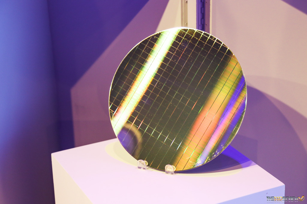
I'm borrowing the above picture from The SSD Review because to be honest my wafer photos (and photos in general) are quite horrible and wafers are far from being the easiest object given all the reflections. Sean is a professional photographer, so he managed to grab this clear and beautiful photo of the production 3D XPoint wafer Intel and Micron had on display, making it easy to estimate the die size.
I calculated 18 dies horizontally and 22 vertically, which yields 227mm^2 with a normal 300mm wafer. When taking die cuts (i.e. the space between dies) into account, we should be looking at 210-220mm^2. Array efficiency is about 90%, which is much higher than planar NAND because most of the peripheral circuitry lies underneath the memory array.
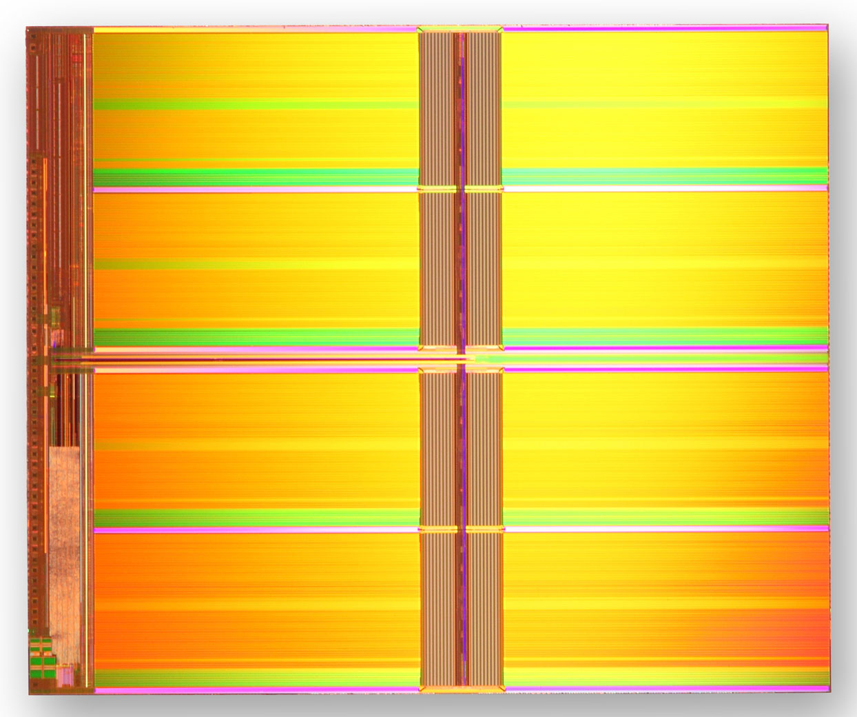
IMFT 20nm 128Gbit MLC NAND die
For comparison, Intel-Micron's 20nm 128Gbit MLC NAND die measures 202mm^2 and has array efficiency of ~75%. From that we can calculate that the 128Gbit memory array in 3D XPoint takes about 190mm^2, while a similar capacity planar NAND array measures ~150mm^2 (since the 128Gbit 3D XPoint die consists of two layers and 128Gbit MLC NAND die stores two bits per cell, the number of layers and bits stored per cell cancel out). It seems like NAND is denser (about 20-25%) from a memory array perspective given a fixed feature size (i.e. lithography), but at this point it's hard to say whether this is due to the cell design itself or something else. Connecting layers of wordlines and bitlines to the intermetal layers likely takes some extra area compared to a 2D process (at least this is the case with 3D NAND), which might partially explain the lower density compared to NAND.
However we will have to wait for some SEM photos to really see what's happening inside the 3D XPoint array and how it compares to NAND in cell size and overall density efficiency. Of course, there is a lot more in total manufacturing cost than just the cell and die size, but I'll leave the full analysis to those with the proper equipment and deeper knowledge of semiconductor manufacturing processes.
What Happens to 3D NAND
The above analysis already gives a hint that 3D XPoint isn't about to replace 3D NAND, at least not in the foreseeable future. That's also what Intel and Micron clearly stated when asked about 3D XPoint's impact on 3D NAND because it's really a new class of memory that fills a niche that DRAM and NAND cannot. The companies are still looking forward to rolling out 3D NAND next year and have a strong roadmap of future 3D NAND generations.
As I mentioned earlier, the way 3D XPoint array is built is quite different from 3D NAND and my understanding is that it's less economical, which is one of the reasons why the first generation product is a two-layer design at 20nm rather than dozens of layers at a larger lithography with single patterning like 3D NAND is. Unless there's a way to build 3D XPoint arrays more like 3D NAND (i.e. pattern and etch multiple layers at the same time), I don't see 3D XPoint becoming cost competitive with 3D NAND anytime soon, but then again it's not aimed to be a NAND successor in short-term.
What happens in ten year's time is a different question, though. 3D NAND does have some inherent scaling obstacles with vanishing string current likely being the biggest and most well known at this point. Basically, the channel in each 3D NAND "cell tower" (i.e. a stack of layers, currently 32 for Samsung and Intel-Micron) is a single string that the electrons have to flow through to reach every individual cell in the string. The problem is that as the length of the string increases (i.e. more layers are added), it becomes harder to reach the top cells because the cells on the way cause disturbance, reducing the overall string current (hence the name "vanishing string current"). For those who are interested in a more detailed explanation of this issue along with some experimental data, I suggest you head over to 3D Incites and read Andrew Walker's post on the topic.
Since most vendors haven't even started 3D NAND mass production, it's not like the technology is going to hit a wall anytime soon and e.g. Toshiba-SanDisk's 15nm NAND has strings consisting of 128 cells, but like any semiconductor technology 3D NAND will reach a scaling limit at some point. Whether that is in five, ten or twenty years is unknown, but having a mature and scalable technology like what 3D XPoint should be at that point is important.


80 Comments
View All Comments
Alexvrb - Friday, July 31, 2015 - link
I don't think so... this is slower than current RAM. They aren't very likely to use HBM only on an APU for various reasons, so you're still going to be using something like DDR4 for your main memory. Which again, is faster than this XPoint tech.XPoint is however a lot denser than RAM, and it's non-volatile so it will make excellent high-speed storage if we can get a better interface. I think in a few years we could at least be using it as a cache for NAND devices or as "boot drives" similar to how we were using then-costly NAND-based SSDs not so long ago.
lilmoe - Monday, August 3, 2015 - link
If we're talking more in a "conventional" non-enterprise, consumer/professional product sense, then I believe this type of memory would be more of a complement to eDRAM (or other forms of higher density, lower speed cache memory), with DRAM completely omitted from the hierarchy. But this may fundamentally change the way operating systems and applications work, and depending on design/application, may lead to breakthrough performance gains.Scoobmx - Friday, July 31, 2015 - link
Ian, I have some serious doubts that this is STT-MRAM. The endurance and density numbers don't really line up. STT has virtually limitless endurance but fairly poor density due to the high current required, hence the need for a large transistor. I don't have the hubris to claim that it's impossible, but I believe it highly unlikely. Source: completed my dissertation in nanomagnetic logic and memory devices last year.J03_S - Friday, July 31, 2015 - link
It might very well be Perpendicular Magnetic Anisotropic Magnetic Tunneling Junction STT-MRAM. It's a variant of STT-MRAM that does not suffer from the density issues and is more than one order of magnitude efficient than Spin torque transfer. It was covered in the AIP journal and published back in April of 2014 by Luc Thomas and associates. At the time they had IBM producing chips for them as the entire process is fully compatible with the existing CMOS backend and requires no special changes be made to the process. This expedited the research quite a bit as they were able to test fully functioning chips.jjj - Friday, July 31, 2015 - link
About the positioning in the market you are being a bit misleading initially.The technology itsalf is likely able to compete with NAND in pricing,there would be a process and layers race but it could be doable.
So it's not really in between NAND and DRAM, cost wise, at least that's not a must, it will cost us a lot more than NAND because Intel and Micron will milk the hell out of it.
About output, that's a startegy matter, the goal being to maximize profits ,nothing else matters. The 2 companies are trying to justify their initial prices and markets by placing it inthe middle- sure it is in the middle perf wise and cost is likely higher for now than the most efficient NAND.
When you comment about power vs NAND you forget to say that it would be per bit and that's kinda relevant.
When you talk about how the laywer are made and costs, it would be important to point out that 3D NAND has very poor planar density compared to 2D NAND. the density here seems to be very close to 2D NAND density. You make it sound like it would cost a lot more than 3D NAND and don't think that's a case at all. Sure maybe it's 2-4 times more than more for now but that's not too far and it's a lot cheaper than RAM. Yes scaling the layers seems costlier here than with 3D NAND.
When talking die size it stops being as misleading as some previous bits. On die size it looks more like 18+ dies and close to 23 so some 13x16mm for 208-ish mm2.
High cell efficiency would be good too when scaling soif they go 16nm 4 layers in gen 2,it would be interesting.
Micron can double it's profits once they max that facility (and Intel takes half) , i was assuming they'll push SSDs at 4-5$ per GB too but i'm sure they'll try to go even higher if they can.
As far as i know PCI 4.0 was due in 2017 so not too far away.
You keep pushing their agenda at the end about where it can go. Look, DDR3 is some 4.5$ per GB, DDR4 getting close to 6.5$ per GB , 128Gb NAND is some 5$ but the range is pretty wide for NAND (3.5-6$). Could they sell it in phones at 1-2$ per GB? Easily, but they won't at first ,it's more profitable not to. Will they do it in gen 2-3, yeah they will. They need to expand it slowly before others have their own 3D ReRAM slutions and have a solid base by that time,whilemaking a lot of money with it in the few years of monopoly.
Ofc in phones they can go for 4-8GB at 3$ per GB and lesser RAM to save power. Don't forget power in phones, just on that and it's worth using a hybrid RAM/ReRAM in high end.
So overall i think you fail to make a clear distinction between the technology and the financial strategy. The big limitation in adoption is the very high margins, the technology itself seems plenty capable and cheap. In IoT could be interesting too when it gets cheap enough but it's not ideal since it's not quite as cheap and dense as the industry would like, a lot more is needed there long term.
Anyway, great that we have this 5 or more years before it was expected, not so great (for us) that it might take a while before prices become accessible for consumers. At least this forces others to accelerate their ReRAM roadmaps.
zodiacfml - Friday, July 31, 2015 - link
Hmm, I think I know why Intel is so invested in this. This will eventually replace NAND drives as performance storage while current NAND drives of today becomes the cold, backup storage replacing the spinning disk drives. I feel that 3D-NAND has more potential for higher density and lower power versus disks. It might become more cost effective or cheaper than hard disks when OEMs starts using NAND in cheap and mid range PCs because of the scale and less buyers of the hard disks.DrKlahn - Friday, July 31, 2015 - link
I think short term you may see Intel and Micron put a small amount of Xpoint as a read/write cache onto their Enterprise and performance oriented SSD's. It would give them a decent performance advantage with a price bump modest enough to still attract consumers.Drumsticks - Friday, July 31, 2015 - link
I've been looking forward to this writeup! I work in NSG at Intel (the Non-Volatile Memory Solutions Group i.e. the people developing 3D XPoint) and we've been super excited for this reveal.It's fun to see the industry analysis, and as always Anandtech has one of the most in-depth!
Vlad_Da_Great - Friday, July 31, 2015 - link
@Drumsticks. Keep the good work, the world is moving thanks to people like you and INTC as a company. Thank you!!!jjj - Friday, July 31, 2015 - link
Forgot to mention that in a promo video they claim SSDs with this would be up to 10x faster over PCIe/NVMe. https://www.youtube.com/watch?t=184&v=Wgk4U4qV...No idea how they do the math ofc so i wouldn't expect 10x random.