The AMD Radeon R9 Fury X Review: Aiming For the Top
by Ryan Smith on July 2, 2015 11:15 AM ESTFiji’s Architecture: The Grandest of GCN 1.2
We’ll start off our in-depth look at the R9 Fury X with a look at the Fiji GPU underneath.
Like the Hawaii GPU before it, from a release standpoint Fiji is not really the pathfinder chip for its architecture, but rather it’s the largest version of it. Fiji itself is based on what we unofficially call Graphics Core Next 1.2 (aka GEN3), and ignoring HBM for the moment, Fiji incorporates a few smaller changes but otherwise remaining nearly identical to the previous GCN 1.2 chips. The pathfinder for GCN 1.2 in turn was Tonga, which was released back in September of 2014 as the Radeon R9 285.

So what does GCN 1.2 bring to the table over Hawaii and the other GCN 1.1 chips? Certainly the most well-known and marquee GCN 1.2 feature is AMD’s latest generation delta color compression technology. Tied in to Fiji’s ROPs, delta color compression augments AMD’s existing color compression capabilities with additional compression modes that are based around the patterns of pixels within a tile and the differences between them (i.e. the delta), increasing how frequently and by how much frame buffers (and RTs) can be compressed.
Frame buffer operations are among the most bandwidth intensive in a GPU – it’s a lot of pixels that need to be resolved and written to a buffer – so reducing the amount of memory bandwidth these operations draw on can significantly increase the effective memory bandwidth of a GPU. In AMD’s case, GCN 1.2’s delta color compression improvements are designed to deliver up to a 40% increase in memory bandwidth efficiency, with individual tiles being compressible at up to an 8:1 ratio. Overall, while the lossless nature of this compression means that the exact amount of compression taking place changes frame by frame, tile by tile, it is at the end of the day one of the most significant improvements to GCN 1.2. For Radeon R9 285 it allowed AMD to deliver similar memory performance on a 256-bit memory bus (33% smaller than R9 280’s), and for Fiji it goes hand-in-hand with HBM to give Fiji an immense amount of effective memory bandwidth to play with.
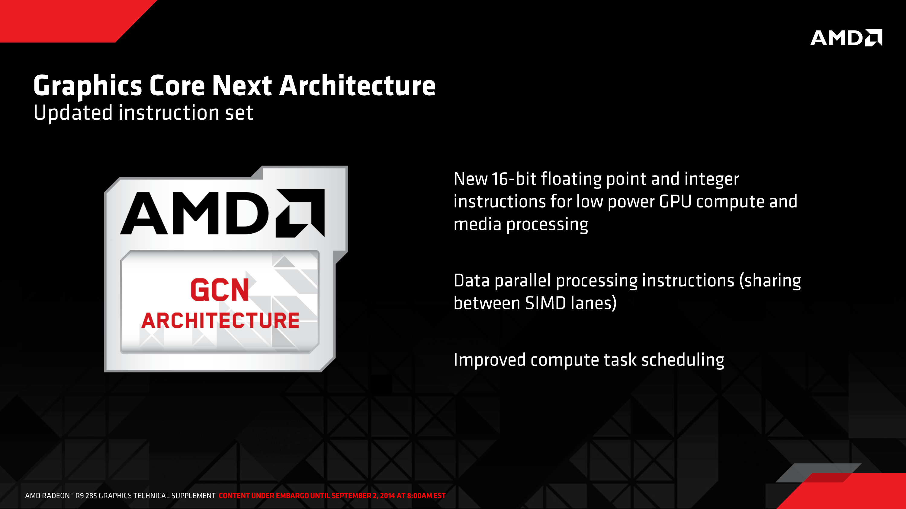
Moving on, AMD has also made some changes under the hood at the ALU/shader level for GCN 1.2. Many of these changes are primarily for AMD’s Carrizo APU, where task scheduling improvements go hand-in-hand with the AMD’s Heterogeneous System Architecture initiative and deliver improvements to allow the CPU and GPU to more easily deliver work to each other. Similarly, 16-bit instructions are intended to save on power consumption in mobile devices that use lower precision math for basic rendering.

More applicable to Fiji and its derivatives are the improvements to data-parallel processing. GCN 1.2 now has the ability for data to be shared between SIMD lanes in a limited fashion, beyond existing swizzling and other data organizations methods. This is one of those low-level tweaks I’m actually a bit surprised AMD even mentioned (though I’m glad they did) as it’s a little tweak that’s going to be very algorithm specific. For non-programmers there’s not much to see, but for programmers – particularly OpenCL programmers – this will enable newer, more efficient algorithms where when the nature of the work requires working with data in adjacent lanes.
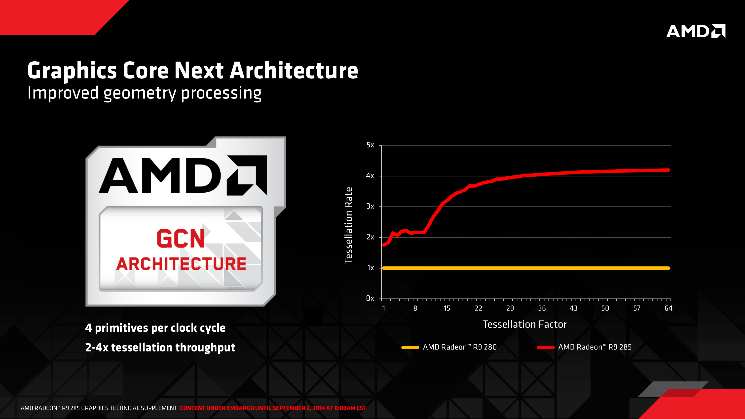
But for gamers, perhaps the most significant architectural improvement to GCN 1.2 and thereby Fiji are the changes made to tessellation and geometry processing. There is no single silver bullet here – after going with a 4-wide geometry front-end in Hawaii, AMD hasn’t changed it for Tonga or Fiji – but AMD has put in quite a bit of effort in to improving how geometry data moves around within the chip and how it’s used, on the basis that at this point the limitations aren’t in raw geometry performance, but rather the difficulties in achieving that performance.
Much of this effort has been invested in better handling small geometry, whether it’s large quantities of small batches, or even small quantities of small batches. The inclusion of small instance caching, for example, allows the GPU to better keep small batches of draw calls in cache, allowing them to be referenced and/or reused in the future without having to go to off-cache memory. Similarly, AMD can now store certain cases of vertex inputs for the geometry shader in shared memory, which like small instance caching allows for processing to take place more frequently on-chip, improving performance and cutting down on DRAM traffic.
More specific to Fiji’s incarnation of GCN is how distribution is handled. Load balancing and distribution among the geometry frontends is improved overall, including some low-level optimizations to how primitives generated from tessellation are distributed. Generally speaking distribution is a means to improve performance by removing bottlenecks, however AMD is now catching a specific edge case where small amplification factors don’t generate a lot of primitives, and in those cases they’re now skipping distribution since the gains are minimal, and more likely than not the cost from the bus traffic is greater than the benefits of distribution.
Finally, AMD has also expanded the vertex reuse window on GCN 1.2. As in the general case of reuse windows, the vertex reuse window is a cache of sorts for vertex data, allowing old results to be held in waiting in case they are needed again (as is often the cases in graphics). Though they aren’t telling us just how large the window now is, GCN 1.2 now features a larger window, which increases the hit rate for vertex data and as a result further edges geometry performance up since that data no longer needs to be regenerated.
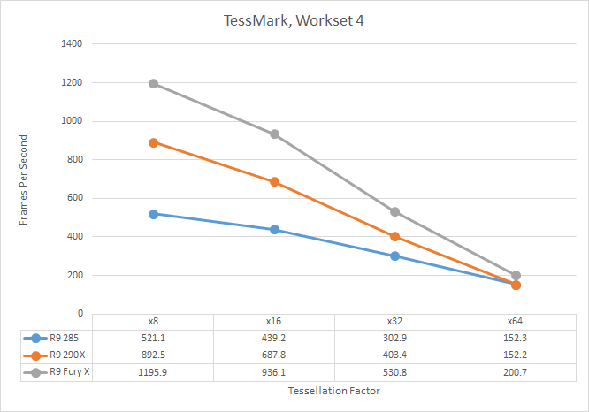
As with our R9 285 review, I took the time to quickly run TessMark across the x8/x16/x32/x64 tessellation factors just to see how tessellation and geometry performance scales on AMD’s cards as the tessellation factor increases. Keeping in mind that all of the parts here have a 4-wide geometry front-end, the R9 285, R9 290X, and R9 Fury X all have the same geometry throughput on paper, give or take 10% for clockspeeds. What we find is that Fury X shows significant performance improvements at all levels, beating not only the Hawaii based R9 290X, but even the Tonga based R9 285. Tessellation performance is consistently 33% ahead of the R9 290X, while against Tonga it’s anywhere between a 33% lead at high factors to a 130% lead at low tessellation factors, showing the influence of AMD’s changes to how tessellation is handled with low factors.


458 Comments
View All Comments
bennyg - Saturday, July 4, 2015 - link
Marketing performance. Exactly.Except efficiency was not good enough across the generations of 28nm GCN in an era where efficiency + thermal/power limits constrain performance, and look what Nvidia did over a similar era from Fermi (which was at market when GCN 1.0 was released) to Kepler to Maxwell. Plus efficiency is kind of the ultimate marketing buzzword in all areas of tech and not having any ability to mention it (plus having generally inferor products) hamstrung their marketing all along
xenol - Monday, July 6, 2015 - link
Efficiency is important because of three things:1. If your TDP is through the rough, you'll have issues with your cooling setup. Any time you introduce a bigger cooling setup because your cards run that hot, you're going to be mocked for it and people are going to be weary of it. With 22nm or 20nm nowhere in sight for GPUs, efficiency had to be a priority, otherwise you're going to ship cards that take up three slots or ship with water coolers.
2. You also can't just play to the desktop market. Laptops are still the preferred computing platform and even if people are going for a desktop, AIOs are looking much more appealing than a monitor/tower combo. So you want to have any shot in either market, you have to build an efficient chip. And you have to convince people they "need" this chip, because Intel's iGPUs do what most people want just fine anyway.
3. Businesses and such with "always on" computers would like it if their computers ate less power. Even if you can save a handful of watts, multiplying that by thousands and they add up to an appreciable amount of savings.
xenol - Monday, July 6, 2015 - link
(Also by "computing platform" I mean the platform people choose when they want a computer)medi03 - Sunday, July 5, 2015 - link
ATI is the reason both Microsoft and Sony use AMDs APUs to power their consoles.It might be the reason why APUs even exist.
tipoo - Thursday, July 2, 2015 - link
That was then, this is now. Now, AMD together with the acquisition, has a lower market cap than Nvidia.Murloc - Thursday, July 2, 2015 - link
yeah, no.ddriver - Thursday, July 2, 2015 - link
ATI wasn't bigger, AMD just paid a preposterous and entirely unrealistic amount of money for it. Soon after the merger, AMD + ATI was worth less than what they paid for the latter, ultimately leading to the loss of its foundries, putting it in an even worse position. Let's face it, AMD was, and historically has always been betrayed, its sole purpose is to create the illusion of competition so that the big boys don't look bad for running unopposed, even if this is what happens in practice.Just when AMD got lucky with Athlon a mole was sent to make sure AMD stays down.
testbug00 - Sunday, July 5, 2015 - link
foundries didn't go because AMD bought ATI. That might have accelerated it by a few years however.Foundry issue and cost to AMD dates back to the 1990's and 2000-2001.
5150Joker - Thursday, July 2, 2015 - link
True, AMD was at a much better position in 2006 vs NVIDIA, they just got owned.3DVagabond - Friday, July 3, 2015 - link
When was Intel the underdog? Because that's who's knocked them down (The aren't out yet.).