The Samsung Exynos 7420 Deep Dive - Inside A Modern 14nm SoC
by Andrei Frumusanu on June 29, 2015 6:00 AM ESTThe Exynos 7420 - Inside a Modern SoC - Continued
An interesting part of the connectivity blocks is the modem connectivity block. Samsung describes this in its drivers as a “Combo PHY” capable of HSIC, PCIe and MIPI LLI. Given the wide range of connectivity options for external modems and the fact that usually there’s only one modem connected in a device, it makes sense to try to consolidate the various standards to save up on die space. The Galaxy S6 comes for the first time with a global rollout of Samsung’s own modem: Shannon 333. The piece which will probably be marketed as Exynos Modem 333, but like the 7420 Samsung has to yet to publicly acknowledge its existence. The company's in-house modems have in the past seen only limited adoption and used mostly in their home market of Korea. Starting with last year’s push of the Galaxy S5 Mini, we saw Samsung for the first time doing a wide-range rollout to other global markets.
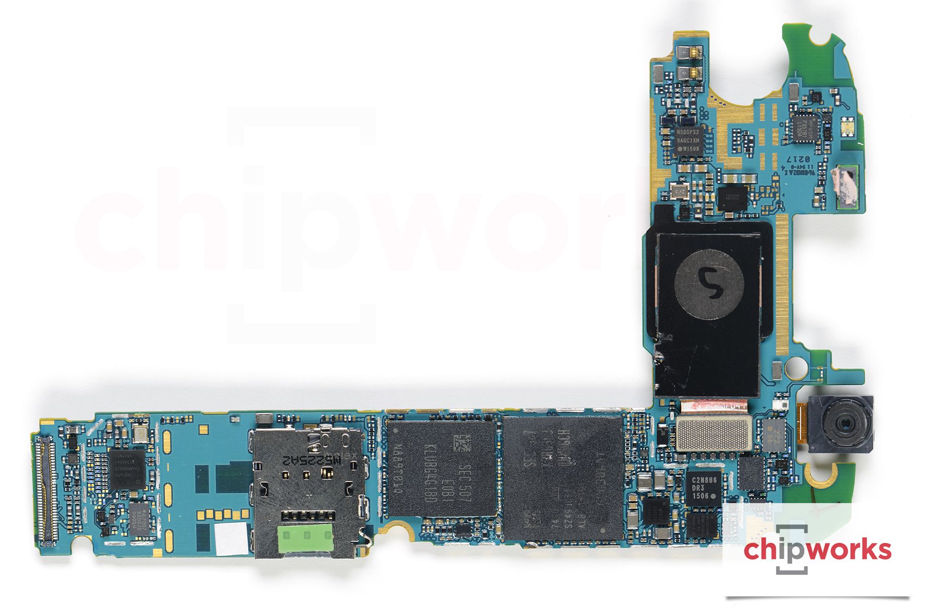
Galaxy S6 PCB with SoC+DRAM and modem+NAND in view. The UFS module sits on top of the modem.
(Image source: Chipworks)
The Shannon 333 is connected to the Exynos 7420 via MIPI LLI (Low Latency Interface). This is an important distinction over past implementations that could have implications on the “integrated vs external” modem discussion. Qualcomm has had an indisputable superiority over competitors due to being able ship an all-in-one solution chipset. The advantage came in two areas: First was due to having a single physical chip; QC had the edge in packaging costs and PCB area footprint. Second one was that external modems require their own dedicated memory to be able to operate. We’ve seen this in many modems in the past, and even Qualcomm’s own Gobi modems such as the MDM9235 need to be partnered with an additional 128MB LPDDR2 of memory. The LLI connection, as opposed to traditional HSIC (High Speed Inter Chip, a USB 2.0 derivative without analog transceivers) interfaces allows the modem to directly access the SoC’s main memory, solving what was one of the most significant overheads of an external modem. Intel was actually the first to have an LLI connected modem in the form of the XMM7260 inside of the Galaxy Alpha, and like the Shannon 333, it was able to ditch the additional memory module which both reduces component cost and power consumption.
While Samsung is unable to comment on this topic, the MIPI Alliance explains that cost and power reduction were the goals of the Low Latency Interface. This also seems to fit with Samsung’s stance on integrated vs dedicated modems, explaining that the latter offers better time-to-market and AP performance characteristics. This makes sense given that modems need regulatory and carrier certifications, a process that takes a lot of money and time. Being able to quickly push out a silicon chip to a production device is critical as the industry now seems desperately to keep up with yearly major refreshes. Also as process nodes get more complex and expensive, it may make sense to actually separate the modem from the main SoC for yield and cost reasons.
It is my opinion that the company will continue with the dual-chip strategy on the high-end, but will still aim to include integrated modems in the low- and mid-range where cost-optimization is absolutely crucial. The Exynos 3470 seen in the Galaxy S5 Mini might see a successor in the ModAP integrated-modem SoC line-up as we’re seeing the first substantial evidence of what the Exynos 7580 is: An 8-core A53 SoC with integrated Shannon 310 modem and LPDDR3 memory. The odd naming convention aside, this looks to be a budget/mid-range chipset aiming to capture some design wins from Qualcomm and MediaTek.
While that was quite a tangent on the modem and its connectivity options, let’s go back to the SoC layout and IP blocks. General connectivity is part of every SoC, and the Exynos 7420 is no different here. With a diverse offering of SPI, HSi2C, UART, i2s, PCM, PWM and other ports it offers all the necessary bus interfaces required to connect all device components to the central SoC. I took the liberty of being very abstract and non-representative with these blocks so one should not read too much into their position or size.
An odd block that I could not account for is a quite larger area next to the A53 cluster. I’m not sure what it represents but it could be an agglomeration of smaller IPs or general SoC logic.
Samsung has used in SoCs previous to the Exynos 5430 a Coarse-Grained Reconfigurable Architecture (CGRA) processing unit called the Samsung Reconfigurable Processor (SRP) for audio processing. The SRP is an interesting architecture that Samsung seems to want to use for a variety of use-cases: We've seen prototype GPUs built with it and Samsung currently uses it as the processing cornerstone of its DRIMe-V SoC in DSLR cameras such as the NX-1. On Exynos SoCs 5430 and newer this audio block was dropped in favour of a more conventional ARM Cortex A5. The companion CPU is in charge of audio decoding, encoding and also audio processing tasks such as equalizer functions. Samsung has previously advertised that it can be also used for voice processing and voice recognition.
Finally, we move on to the media quadrant of the SoC. Here we find the ISP, the hardware media decoder/encoder and the display pipelines.
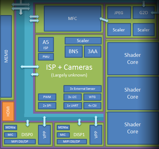
This part of the SoC is depicted totally different than the actual physical layout.
The Exynos’s hardware media accelerator is called the Multi-Format-Codec (MFC). This is a mature block as it has seen implementation in SoCs since the S3C6400 in 2007. Despite being out in the wild for 8 years now, we still don't know much at all about the architecture of the block. My assumption is that we’re most likely looking at a custom DSP architecture as the piece is accompanied by separate firmware that needs to be loaded for operation. The IP is able to encode and decode MPEG4, H263, H264, VP8, and HEVC and can additionally decode MPEG2, VC1 and VP9. The Exynos 5430 and 5433 used an additional HEVC decoder block separate of the MFC to be able to enable playback of the format, but with the 7420 this piece has been subsequently retired from the SoC as its functionality has been merged into the MFC.
I’ve always been impressed with Samsung’s hardware decoder in terms of performance and power, and the v9 of the MFC in the in the 7420 is no exception. I was able to playback 4Kp30 Main HEVC at only about 950mW of total device power (Minimum brightness, portrait mode to try to compensate for display power). This represents about only 600mW of system load power. The CPU load was very low as it hovered around 25-30% at 400MHz on two A53 cores. Unfortunately the decoder isn’t capable of Main10 profile (10bit) playback and freezes up after 2 seconds of 4Kp60 playback, making it not as future-proof as one would have hoped. As a note, Qualcomm’s Snapdragon 810 decode unit has the same limitations, so the playing field for this generation between the two major vendors is even.
Among the collection of media related blocks we find the ISP. We know very little about Samsung’s ISP, but it certainly is a very advanced piece of IP as Samsung can fall back to experience gained not only in the mobile sector but also in the standalone camera market where it produces its custom line of camera SoCs. The ISP consists of a mix of general purpose blocks such as a Cortex A5 running at 668MHz in tandem with a variety of fixed-function units.
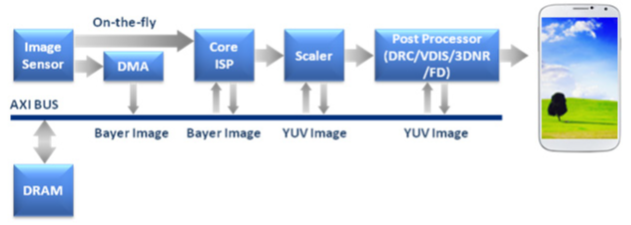
Source: Samsung
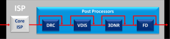
Most that we know about the ISP architecture is from a 2013 paper Samsung had published on the Exynos 5420’s capabilities. There they explain that the whole ISP is formed by a series of sub-IPs each having their specialized jobs, such as sensor defect compensation, 3A (Auto-focus, Auto-exposure, Auto-white-balance), de-mosaic, inter-frame noise-reduction, phase-detection auto-focus, gyro digital image stabilizer, optical lens correction, face-detection, video stabilizer, and probably an even longer list of image processing features we’re not aware of. The SoC has 4 CSI ports and seems to have support for 3 image sensors.
Finally, we move on to the display pipeline, which Samsung calls DECON, short for Display and Enhancement Controller. The DECON block is also responsible for hardware layer composition. Mobile devices use hardware layers – meaning different frame-buffers on which they draw content to, and let the hardware unit recombine them into the final image. The most common example of this is the Android status bar window. Instead of having to re-render the whole screen whenever there’s activity on the status bar, the system will just redraw the thin status bar and let the hardware units do the composition. Video playback windows and application overlays work in a similar fashion.
The SoC has two main display controllers besides a separate HDMI output. Each is capable of MIPI DSI or DisplayPort output, although I’m not sure what its full capabilities such as resolution and frame-rate are. One addition to the Exynos 7420 that wasn’t present before in past variants is a Video Post-Processor (VPP) on each display controller. I’m again uncertain what the new block does but it seems to be capable of color-space conversions and uses poly-phase filters for a some certain task. Also part of each display controller is a block called MDNIe (Mobile Digital Natural Image Enhancement) which is used on all Exynos SoC for image color manipulation, sharpening and a large number of other effects. This is the block that enables Samsung devices to have different display profiles targeting different calibrations. As a side note, Samsung also employs a similar block on their external AMOLED DDICs to provide functionality to third-party SoCs in devices not using Exynos.
I’ve covered a bit what MIC (Mobile Image Compression) was able to provide to the Galaxy Note 4 in our review of that device; Display resolutions higher than 1080p make the image bandwidth required to transmit data from the SoC to the DDIC exceed the capacity of usual 4-lane MIPI DSI interfaces. To able to drive 1440p and higher displays vendor are either required to double up on the interface to a dual-DSI configuration, effectively using 8 lanes and thus doubling the power consumption of such an implementation. The alternative is to go the route of compressing the stream. Currently Samsung is the only one to offer such a solution in the form of their proprietary MIC mechanism, as the up-and-coming industry standard DSC (Display Stream Compression) has not yet seen compatible products released.
An interesting feature of both implementations that I previously wasn’t familiar with is the capability of doing partial slice updates. This means that if only a smart part of the screen is updated, then the compression algorithm only updates and transmits that part of the image, saving even more power by cutting down redundant data transmissions. I could verify this by changing and exaggerating the image color parameters via the MDNIe block. The display controller wouldn’t explicitly refresh the whole image after changing the color configuration, and only issue a slice update to the DDIC when the clock and WiFi-indicator showed activity. Due to the partial update, only a very small part of the screen would update with the new colors, demonstrating that the SoC transmits only fractions of screen data as static content is buffered directly on the DDIC.
Overall, the Exynos 7420 is an interesting SoC and I hope we’ve been able to better shed some light into most of the significant IP blocks that go into a modern SoC. At 78mm² the 7420 has quite some headroom to grow to the usual size of a high-end SoC. It’s possible Samsung intentionally kept the chip small to get more yield and higher unit volume as it is the first 14nm mass-production chipset for their foundries. It’s also possible that as the $/transistor metric hasn't gone down 14nm FinFET due to it being a very expensive process, that we’re seeing the start of a new trend and the end of large 100mm²+ SoCs. It’ll definitely be interesting to see in what direction the mobile semiconductor vendors will be heading in the coming year as the process gains maturity and production volume further ramps up as Samsung expands and GlobalFoundries and TSMC start their own FinFET mass-production.


114 Comments
View All Comments
Andrei Frumusanu - Monday, June 29, 2015 - link
Frankly, I don't know. I tried to ask Samsung a similar question but they refused to comment on customer relations. Meizu so far seems to be the only major vendor consistently using Exynos parts but as to why we haven't seen other vendors adopt them can be attributed to anything going from pricing to volume availability. Only the companies themselves know the details of these contracts.gnx - Monday, June 29, 2015 - link
Thanks! The SoC market is really strange.id4andrei - Monday, June 29, 2015 - link
This is Samsung's chance to eat Qualcomm's lunch. Close down node manufacturing for others(including Apple) and be like Intel. Either use Exynos or be satisfied with inferior nodes from other fabs.CiccioB - Monday, June 29, 2015 - link
And that meas start competing with PP only, like Intel did.That is, if you force others to go to other foundries, you have to be sure you have the best one, or in case TMSC comes up with a better PP (like a 16+nm revision) you have just thrown all your customers to your fab competitors, making double damage (or total one). Or just think if Intel tomorrow suddenly opens to ARM customers in order to saturate it's now rusting 14nm machineries. Samsung would be in great trouble after that eventual (and IMHO stupid) move.
Investing in PP i really expensive and there are other foundries capable of doing so. Samsung can't be sure to always be the best one on the market. And invest tons of billions of dollar every year to make sure to be the number one (for SoC of course).
ZeDestructor - Wednesday, July 1, 2015 - link
Samsung is part of a common platform alliance/agreement with GloFo, so while they could lock down and close others out, GloFo would not, so there's little commercial benefit from doing so.They could of course coerce GloFo into doing the same, but that lands them into hot water with regulatory watchdogs like the FTC regarding anti-competitive practices and collusion, which while Samsung wouldn't really mind (no, really), GloFo would.
eh_ch - Monday, June 29, 2015 - link
How will it take for Samsung's process to trickle down to AMD via GloFo? Could it bridge the efficiency gap to nvidia / Intel? Holding out hope that ATI/MD will be competitive once more.eh_ch - Monday, June 29, 2015 - link
How long will it take, that isAdding-Color - Monday, June 29, 2015 - link
No, AMD won't have a technology advantage to Nvidia on next gen GPUs, currently it looks like nvidia will choose Samsung for their next node, and as Samsung and GloFo jav some kind of alliance and share processes (glofo licenses some Samsung processes AFAIK, the technology should be very similar for both, yet AMD should have a small HBM advantage, they have better relations to hynix (and helped to develop HBM) than nvidia.jjj - Monday, June 29, 2015 - link
There won't be a HBM advantage from a technological point of view, at best AMD could get slightly better pricing but even that is unlikely since Nvidia has much higher volume. The first gen HBM was late and both Nvidia and AMD had plenty of time to prepare for it.As for the process, we don't really know what foundry each will use and what version of the process.On the GPU side both are more likely to go TSMC or use both. On the CPU side AMD will likely go GloFo but not this early version of the process and Intel might go 10nm not long after AMD has 14nm. On 10nm TSMC and Samsung do seem to be catching up with Intel but doubt AMD will have 10nm early.
fluxtatic - Tuesday, June 30, 2015 - link
Hell, at this point I'd be happy to see AMD at < 28nm