The Samsung Exynos 7420 Deep Dive - Inside A Modern 14nm SoC
by Andrei Frumusanu on June 29, 2015 6:00 AM ESTWe move on to our benchmarking sections with the CPU’s performance and power consumption. We have already extensively covered ARM’s A5x CPU architectures in our detailed review of the Exynos 5433, and interested readers should definitely have a read of that piece if they want to get a good grasp of how ARM’s CPUs in the SoCs were designed. The Exynos 7420 is identical to the 5433 in terms of CPU configuration: We still have four A53 cores and four A57 cores connected by the CCI-400 interconnect. The only difference is in the clock speeds as Samsung now pushes the frequency slightly higher at 1.5GHz and 2.1GHz for the little and big clusters.
CPU Performance: 64-bit Processing
One interesting benchmark that we weren’t able to measure on the Exynos 5433 due it still coming with a 32-bit software stack was the AArch64 performance of the CPUs. To have a look at the impact 64-bit code has on the device we use SPECint2000 compiled for both 32 and 64bit targets on the Exynos 7420. The scores are estimated results and should in not be considered representative of the device’s performance and only show an architectural view of the CPUs performance.
Developed by the Standard Performance Evaluation Corporation, SPECint2000 is the integer component of their larger SPEC CPU2000 benchmark. Designed around the turn of the century, officially SPEC CPU2000 has been retired for PC processors, but mobile processors are roughly a decade behind their PC counterparts in performance. Keeping that in mind it still provides an excellent benchmark for today's mobile phones and allows us to do single-threaded architectural comparisons between the competing CPU designs out there. The scores we publish are only estimates and should not taken as officially validated numbers.
| SPECint2000 base - Estimated Scores Little Cores |
||||||
| Exynos 5433 (Cortex A53) AArch32 |
Exynos 7420 (Cortex A53) AArch32 |
Exynos 7420 (Cortex A53) AArch64 |
Exynos 7420 64 > 32 bit % Advantage |
|||
| 164.gzip | 396 | 432 | 496 | 15% | ||
| 175.vpr | 272 | 290 | 283 | -2% | ||
| 176.gcc | 597 | 674 | 2000 | 197% | ||
| 181.mcf | 291 | 300 | 248 | -17% | ||
| 186.crafty | 448 | 492 | 343 | -30% | ||
| 197.parser | 348 | 373 | 360 | -3% | ||
| 252.eon | 935 | 1092 | 1354 | 24% | ||
| 253.perlbmk | 529 | 588 | 3000 | 410% | ||
| 254.gap | 544 | 611 | 1506 | 146% | ||
| 255.vortex | 529 | 552 | 627 | 14% | ||
| 256.bzip2 | 362 | 395 | 426 | 8% | ||
| 300.twolf | 284 | 306 | 297 | -3% | ||
Starting off with the A53’s performance benefit (or deficit) for AArch64 code, we see a weird phenomenon as the 64-bit results not always outperform the 32-bit variant of the benchmark. Depending on the sub-test, we’re seeing the effect of having to work with 64-bit integers. Tests such as mcf or crafty visibly suffer from the move as the CPU internally has to deal with larger data sizes. There is increased pressure on the caches which slows down the computation speed in these tests. On the other hand, we have other sub-tests which show very large improvements such as gcc, perlbmk and gap as they are able to take advantage of 64-bit registers and other ISA changes for computational purposes. Running such pieces of code brings 2-4x the speedup on the A53 core.
| SPECint2000 base - Estimated Scores Big Cores |
||||||
| Apple A8 (Typhoon) AArch64 |
Exynos 5433 (Cortex A57) AArch32 |
Exynos 7420 (Cortex A57) AArch32 |
Exynos 7420 (Cortex A57) AArch64 |
Exynos 7420 64 > 32 bit % Advantage |
||
| 164.gzip | 842 | 813 | 909 | 927 | 2% | |
| 175.vpr | 1228 | 1120 | 1129 | 1014 | -10% | |
| 176.gcc | 1810 | 1549 | 1617 | 2000 | 24% | |
| 181.mcf | 1420 | 1192 | 1276 | 923 | -28% | |
| 186.crafty | 2021 | 1149 | 1282 | 990 | -23% | |
| 197.parser | 1129 | 841 | 904 | 895 | -1% | |
| 252.eon | 1933 | 2096 | 2280 | 2500 | 10% | |
| 253.perlbmk | 1666 | 1258 | 1363 | 4000 | 193% | |
| 254.gap | 1821 | 1466 | 1506 | 3437 | 128% | |
| 255.vortex | 1716 | 1652 | 1596 | 1681 | 5% | |
| 256.bzip2 | 1234 | 1027 | 1102 | 1102 | 0% | |
| 300.twolf | 1633 | 1260 | 1428 | 1875 | 31% | |
Moving on to the A57 numbers, we again see a similar scenario as the 64-bit vpr, mcf, and crafty show a significant performance downgrade compared to the 32-bit variants due to higher memory and cache pressure. Perlbmk and gap are again the largest benefactors of 64-bit register usage. While the performance boost for the gcc compiler test was significant for the A53 cores, the A57 cores come in at a less impressive but still respectable 28% performance boost.
Overall it’s interesting to see what kind of an impact AArch64 has on performance and it’s clear that the advantages are very architecture and use-case dependent. The two most negatively affected benchmarks were 181.mcf and 186.crafty. The former is based on a single-depot vehicle scheduling algorithm with almost exclusive integer arithmetic that doesn’t take advantage of 64-bit data-structures, so most of performance is wasted due to overhead.
The Galaxy S6 most-notably still employs a 32-bit native browser, and although I'm not sure if this was a deliberate decision or carry-over from existing firmwares, this may be a sign that it may not always be worth to switch over to AArch64 compiled applications.
Memory Latency and Performance
LPDDR4 is one of the major specification upgrades for many high-end 2015 SoCs and the 7420 is along with the Snapdragon 810 one of the first mobile SoCs to adopt the new technology. LPDDR4 doubles its operational frequency over LPDDR3, and the Exynos 7420 runs its memory at 1555MHz (3110MT/s). In terms of computational requirements, CPUs are more sensitive to latency while GPUs require more bandwidth to operate at the best efficiency. As a start, we’ll look at how memory latency has changed on the Exynos 7420. For this review I choose to present the results on a logarithmic scale to better depict the latency differences on the L1 and L2 caches.

The A53 cores don’t show any significant variation in the L1 and L2 results that exceeds the expected 15% difference due to the higher clock-speed of the Exynos 7420’s little cores. As transfer size grows beyond 256kB we see our benchmark leaving pre-fetching and caching on the L2 and hit main memory. Here the Exynos 7420 sees a rise in latency to 206ns over the 5433’s 191ns.
The change in main memory latency is also visible in the bandwidth results of the 7420’s little cores as transfer speeds overall drops on average 10% over what we’ve measured on the 5433.

The latency graphs for the big cores looks more interesting as we see a quite large difference in the L1 cache of the Exynos 7420. The new chip is able to offer a 76% improvement in the L1 latency when compared to the Exynos 5433, as the new SoC is able to hold a very steady 1.91ns versus an average 3.36ns on the predecessor A57 implementation. The frequency advantage of the 7420 comes in at only 10%, so Samsung definitely must have made some changes in the cache architecture as I was able to measure much more consistent latency and bandwidth results in our custom benchmark.
The bandwidth results on the L1 and L2 caches are equally significant: The L1 bandwidth improved on average by 89% while the L2 also saw a 46% increase over the Exynos 5433. NEON load instructions in particular seem have gotten a very large improvement as we’re able to measure a 2.4-3.1x bandwidth boost on the L2 and L1 caches compared to the Exynos 5433’s A57 cluster.
The latency and bandwidth differences are smaller when hitting main memory. The A57 cluster on the new chip actually does better than the 5433 as main memory latency slightly improves by 8ns to 172ns, which results in the same average 4% boost in memory bandwidth using various common access methods. The CPU's are certainly not limited by main memory as they're far from saturating the bus bandwidth on the CCI. As previously mentioned in the SoC layout section, Samsung chooses to limit the CCI to 532MHz instead of going higher to match DRAM speeds. This is contrary to other SoCs and Qualcomm's Snapdragon 810 which runs the CCI at up to 787MHz.
All in all, it seems Samsung may have done some optimizations on the A57 cores that manage to significantly improve their memory performance. One could reason that any performance improvements exceeding the 10% / 200MHz frequency boost, and not affected by possible AArch64 instruction set usage may be result of the higher on-core and cluster cache performance boost, and while that’s hard to verify, we see no other architectural difference between the 7420 and its predecessor.
Off-topic - Galaxy S6 Disassembly Process
Before I get into the power numbers and explain our methodology, I would like to take the opportunity to share my experience with dismantling the Galaxy S6 and getting access to the battery, as some readers and eventual device owners might be interested to hear about the feasibility of the battery swapping process. The by far most daunting process and time-consuming procedure is the removal of the glass back-cover.
The Gorilla Glass 4 piece is held in place by very heavy-duty glue surrounding the edges of the device. It’s basically required to have a very strong suction cup and at least a hair dryer if one doesn’t have access to a heat gun. I used a car's GPS mount for the suction cup as it provided a tight hold and also acted as a lever to pull on. The glue needs to reach a high temperature to soften up, and you might need to heat up (along the edge) the device until it’s no longer comfortable or possible to hold. One should have some plastic picks ready – I just cut up a plastic SIM-card holder into pieces to use them as picks. The initial prying should start at the bottom of the device opposite of the speaker. The process takes a lot of force before one is able to put the first pick in and it definitely not for the faint-of-heart. Slowly advancing along the edge of the device with repeated re-heating should get you to remove the glass cover from the main body.
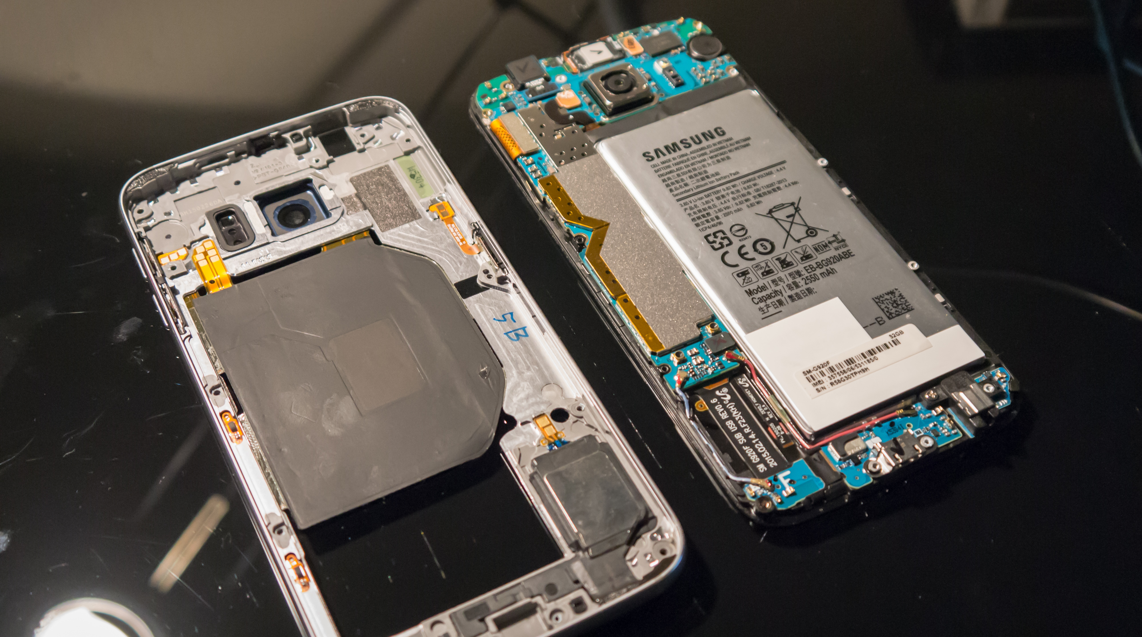
Once the back cover is removed, the rest of the process is very easy as we’re just dealing with ordinary Phillips screws. After removing all visible screws one should apply moderate heat along the front edges of the display. While keeping pressure on the battery one lifts up the whole unibody frame of the device from the screen and motherboard assembly. For the normal Galaxy S6 the process is almost over as the battery is now in direct view and accessible, one can disconnect the connector and slowly and carefully pry it up from the sides to separate it from being glued on the display assembly. S6 Edge owners will require further removing of the motherboard as the battery connector wraps around to the back of the PCB.
Once the new battery is in place and properly connected, the re-assembly process becomes straightforward as it is just a reversal of the disassembly steps. One should make sure that the glue strips on the glass back cover don’t have ridges or overlapping pieces as it will cause the back cover to slightly stick out and no longer be level with the metal frame. Once the phone is back together, I would again recommend applying heat along the edges of the device while forcibly squeezing the back glass and whole assembly back in place.
Overall, the whole procedure of replacing the battery should take up to 30-40 minutes depending how much one struggles to remove the back glass. We’ll have to see how Samsung's new battery chemistry holds up after 1 year of constant usage and fast-charge cycles, but if required to swap out the battery it’s definitely a doable process if one manages to muster up the initial courage.


114 Comments
View All Comments
jjj - Monday, June 29, 2015 - link
The power doesn't look that great, for the A57 seems to allow 300-350Mhz higher clocks, granted it's not a clean shrink. It looks good here because on 20nm they pushed the clocks way high.name99 - Monday, June 29, 2015 - link
Insofar as rumors can be believed, the bulk of A9's are scheduled to be produced by Samsung, presumably on this process. It seems strange to have Apple design/layout everything twice for the same CPU, so if these same rumors (30% going to TSMC) are correct, presumably that means the A9X will be on TSMC.As for characterizing Apple CPUs, while there are limits to what one can learn (eg in the voltage/power tradeoffs), there is a LOT which can be done but which, to my disappointment, has still not been done. In particular if someone wanted, I think there's scope for learning an awful lot from carefully crafted micro benchmarks. Agner Fog has give a large number of examples of how to do this in the x86 space, while Henry Wong at stuffedcow.net has done the same for a few less obvious parts of the x86 architecture and for GPUs.
It strikes me as bizarre how little we know about Apple CPUs even after two years.
The basic numbers (logical registers, window, ROB size) seem to about match Intel these days, and the architecture seems to be 6-wide with two functional clusters. There appears to be a loop buffer (but how large?) But that's about it.
How well does the branch prediction work and where does it fail?
What prefetchers are provided? (at I1, D1, L2. L3)
Do the caches do anything smart (like dead block prediction) for either performance or power?
Does the memory manager do anything smart (like virtual write queue in the L3)?
etc etc etc
Obviously Apple doesn't tell us these. (Nowadays the ONLY company that does is IBM, and only in pay-walled articles in their JRD.) But people write the micro benchmarks to figure this out for Intel and AMD, and I wish the same sort of enthusiasm and community existed in the ARM world.
SunnyNW - Wednesday, July 1, 2015 - link
Believe word on the street is the A9 will be Sammy 14nm and the A9X TSM 16nm+SunnyNW - Wednesday, July 1, 2015 - link
Please ignore this comment, should have read the rest of the comments before posting since Name99 already alluded to this below. SorryCiccioB - Monday, June 29, 2015 - link
Is the heterogeneous processing that allows all 8 cores working together active?Seen the numbers of the various bench it seems this feature is not used.
What I would like to know exactly is that is the bench number of this SoC can be directly compared to SoC with only 4 cores like the incoming Qualcomm Snapdragon 820 based on custom architecture which has "only" 4 cores and not a big.LITTLE configuration.
Andrei Frumusanu - Monday, June 29, 2015 - link
HMP is active. Why do you think it seems to be not used?CiccioB - Monday, June 29, 2015 - link
Because with 8 cores active (or what they should be with HMP) results is not even near 4x the score of a single core.So I wonder if those 8 core are really active. And whether they are of any real use if, to keep consumption adequate, frequencies of higher cores get limited.
Andrei Frumusanu - Monday, June 29, 2015 - link
All the cores are always active and they do not get limited other than in thermal stress situations. I didn't publish any benchmarks comparing single vs multi-core performance so your assumption must be based on something else. Having X-times the cores doesn't mean you'll have X-times the performance, it completely depends on the application.It's still a perfectly valid comparison to look at traditional quad-cores vs bL octa-cores. In the end you're looking at total power and total performance and for use-cases such as PCMark the number of cores used shouldn't be of interest to the user.
Refuge - Monday, June 29, 2015 - link
I would hazard a guess that thermal throttling has something to do with part of it.ruturaj1989@gmail.com - Monday, June 29, 2015 - link
It does have 4 cores but I guess they are in big.LITTLE configuration too. We will see shortly. HMP is active but I am not sure if every bench app uses all the cores.