AMD Launches Carrizo: The Laptop Leap of Efficiency and Architecture Updates
by Ian Cutress on June 2, 2015 9:00 PM ESTThe Platform
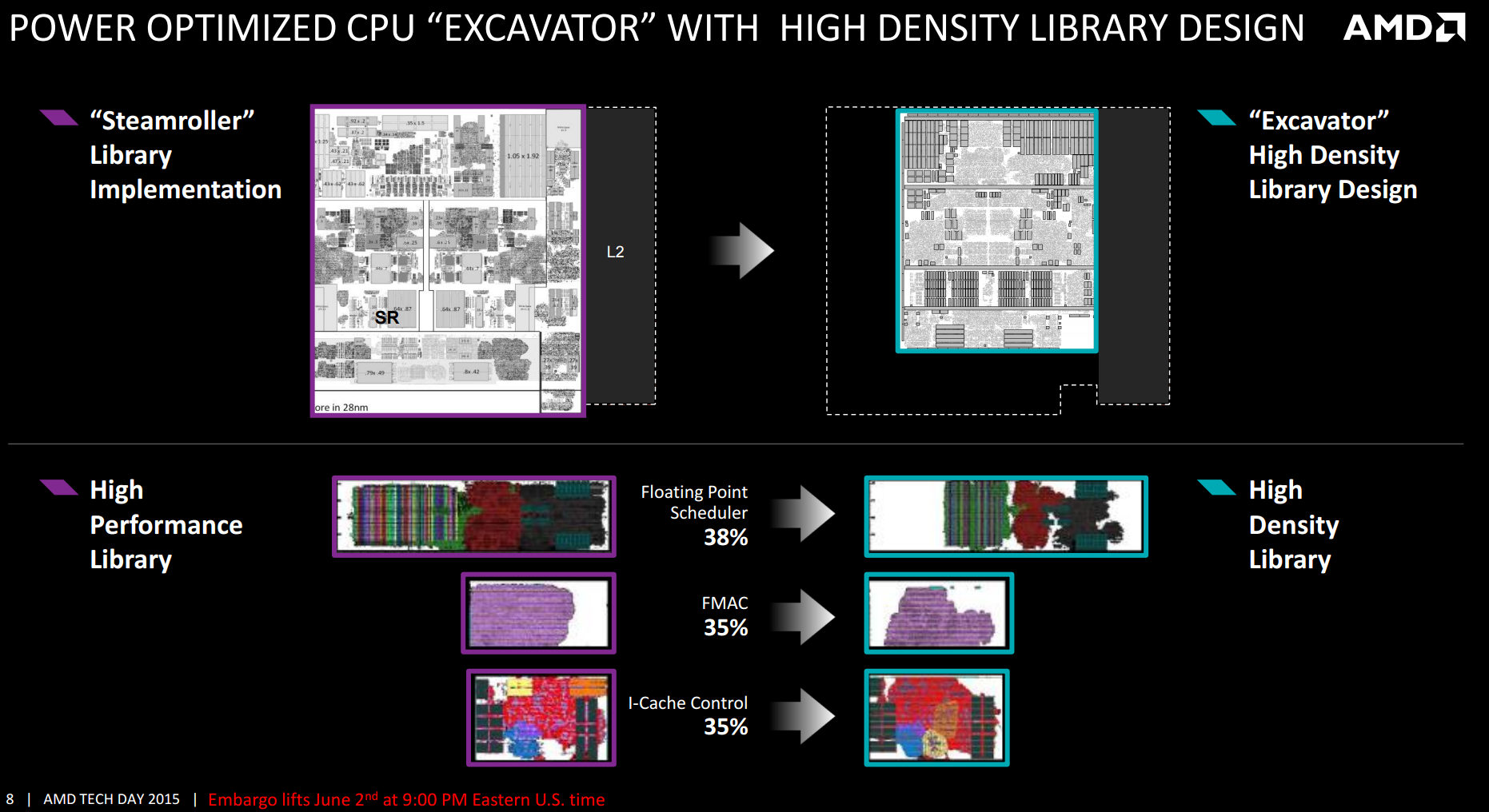
From a design perspective, Carrizo is the biggest departure to AMD’s APU line since the introduction of Bulldozer cores. While the underlying principle of two INT pipes and a shared FP pipe between dual schedulers is still present, the fundamental design behind the cores, the caches and the libraries have all changed. Part of this was covered at ISSCC, which we will also revisit here.
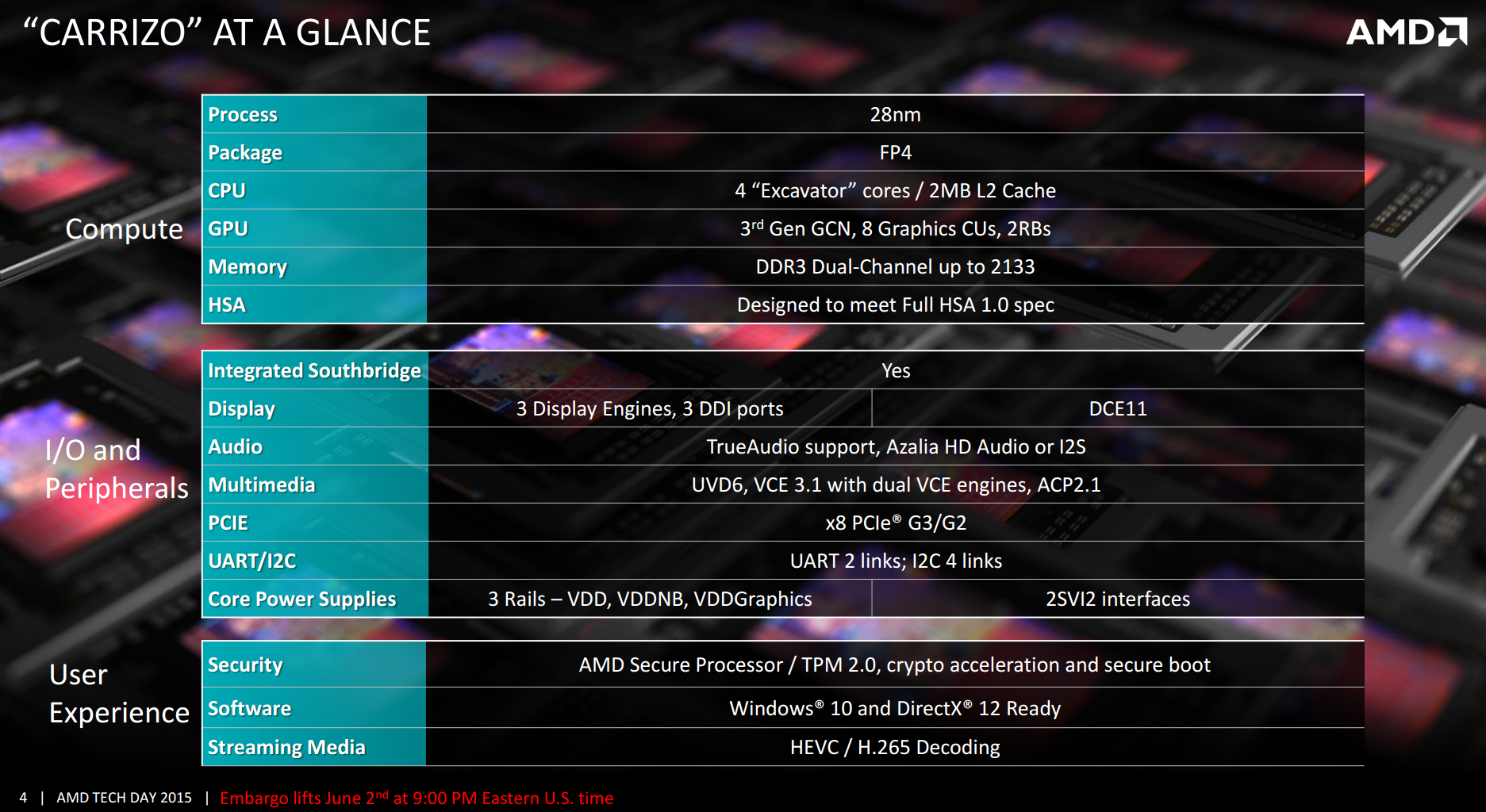
On a high level, Carrizo will be made at the 28nm node using a similar silicon tapered metal stack more akin to a GPU design rather than a CPU design. The new FP4 package will be used, but this will be shared with Carrizo-L, the new but currently unreleased lower-powered ‘Cat’ core based platform that will play in similar markets for lower cost systems. The two FP4 models are designed to be almost plug-and-play, simplifying designs for OEMs. All Carrizo APUs currently have four Excavator cores, more commonly referred to as a dual module design, and as a result the overall design will have 2MB of L2 cache.
Each Carrizo APU will feature AMD’s Graphics Core Next 1.2 architecture, listed above as 3rd Gen GCN, with up to 512 streaming processors in the top end design. Memory will still be dual channel, but at DDR3-2133. As noted in the previous slides where AMD tested on DDR3-1600, probing the memory power draw and seeing what OEMs decide to use an important aspect we wish to test. In terms of compute, AMD states that Carrizo is designed to meet the full HSA 1.0 specification as was released earlier this year. Barring any significant deviations in the specification, AMD expects Carrizo to be certified when the final version is ratified.
Carrizo integrates the southbridge/IO hub into the silicon design of the die itself, rather than a separate on package design. This brings the southbridge down from 40nm+ to 28nm, saving power and reducing long distance wires between the processor and the IO hub. This also allows the CPU to control the voltage and frequency of the southbridge more than before, offering further potential power saving improvements. Carrizo will also support three displays, allowing for potentially interesting combinations when it comes to more office oriented products and docks. TrueAudio is also present, although the number of titles that support it is few and the quality of both audio codecs and laptop speakers leaves a lot to be desired. Hopefully we will see the TrueAudio DSP opened up in an SDK at some point, allowing more than just specific developers to work with it.
External graphics is supported by a PCIe 3.0 x8 interface, and the system relies on three main rails for voltage across the SoC which allows for separate voltage binning of each of the parts. AMD’s Secure Processor, with cryptography acceleration, secure boot and BitLocker support are all in the mix.


137 Comments
View All Comments
name99 - Saturday, June 6, 2015 - link
You are comparing a $400 laptop to a $1500 laptop and, what do you know, the $1500 laptop comes out better. What a surprise!The point is that in this space batteries have long been cheap and the energy efficiency nothing like at the higher end. Which means the work-life has been something like 3 hrs. If AMD shifts that to six hours with this chip, that's a massive improvement in the target space.
You're also making bad assumptions about why these laptops are bought. If you rely on your laptop heavily for your job, you buy a $1500 laptop. These machines are bought to act as light performance desk machines that are occasionally (but only occasionally) taken to a conference room or on a field trip.
name99 - Saturday, June 6, 2015 - link
AMD does not have infinite resources. This play makes sense.Intel is essentially operating by starting with a Xeon design point and progressively stripping things out to get to Broadwell-M, which means that Broadwell-M over-supplies this $400-$700 market. Meanwhile at the really low end, Intel has Atom.
AMD is seeing (correctly, I think) that there is something of a gap in the Intel line which they can cover AND that this gap will probably persist for some time --- Intel isn't going to create a third line just to fit that gap.
Krysto - Wednesday, June 3, 2015 - link
I might be ready to get into AMD, as AMD has a lot of innovation lately. But it still disappoints me greatly that they aren't able to adopt a more modern process node.If they launch their new high-performance CPU core next year as part of an APU that uses HBM memory and is at the very least on 16nm FinFET, I might get that instead of a Skylake laptop. HSA is pretty cool and one of the reasons I'd get it.
UtilityMax - Wednesday, June 3, 2015 - link
The Kaveri FX parts are still almost half as slow in IPC as a competing Intel Core i3 with the same TDP. Only in tests involving multithreaded apps that can load all four cores the FX parts are keeping up with the Core i3. Let's hope the Carrizo generation of APUs will improve this situation.silverblue - Thursday, June 4, 2015 - link
Without being an AMD apologist, I think the point was that single threaded performance was "good enough" for your usual light work which tends to be hamstrung by I/O anyway.There are two things that I need to see clarified about Carrizo, however:
1) Does Carrizo drop CPU frequency automatically when the GPU is being taxed? That's certainly going to be an issue as regards the comparison with an i3.
2) With the addition of AVX2, were there any architectural changes made to accommodate AVX2, for example a wider FlexFPU?
sonicmerlin - Tuesday, June 9, 2015 - link
Yup. I'll wait for the 14 nm Zen APUs with HBM. The performance leap (both CPU and GPU) should be truly massive.Phartindust - Thursday, June 4, 2015 - link
Dude your gettin a Dell with a AMD processor!When was the last time that happened?
Looks like @Dell loves #Carrizo, and will use @AMD once again. #AMDRTP http://www.cnet.com/au/news/dell-inspirion-amd-car... …
elabdump - Friday, June 5, 2015 - link
Don't forget that Intel gives you an non fixable NSA approved BIOS: http://mjg59.dreamwidth.org/33981.htmlpatrickjchase - Friday, June 5, 2015 - link
Ian, you appear to have confused I-cache and D-cache.You wrote: "The L1 data cache is also now an 8-way associative design, but with the better branch prediction when needed it will only activate the one segment required and when possible power down the rest".
This is of course gibberish. Branch prediction would help to predict the target set of an *instruction* fetch from the I-cache, but is useless for D-cache set prediction for the most part (I say "for the most part" because Brad Calder did publish a way-prediction scheme based on instruction address back in the 90s. It didn't work very well and hasn't been productized that I know of).
zodiacfml - Friday, June 5, 2015 - link
Imagine what they could with 14nm of this, probably at half the cost of a Core M with 60 to 70% CPU performance of the M, yet with better graphics at the same TDP.