AMD Launches Carrizo: The Laptop Leap of Efficiency and Architecture Updates
by Ian Cutress on June 2, 2015 9:00 PM ESTThe Platform
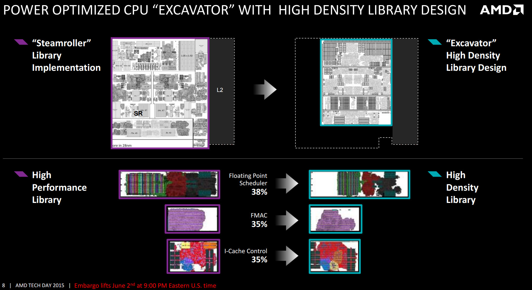
From a design perspective, Carrizo is the biggest departure to AMD’s APU line since the introduction of Bulldozer cores. While the underlying principle of two INT pipes and a shared FP pipe between dual schedulers is still present, the fundamental design behind the cores, the caches and the libraries have all changed. Part of this was covered at ISSCC, which we will also revisit here.
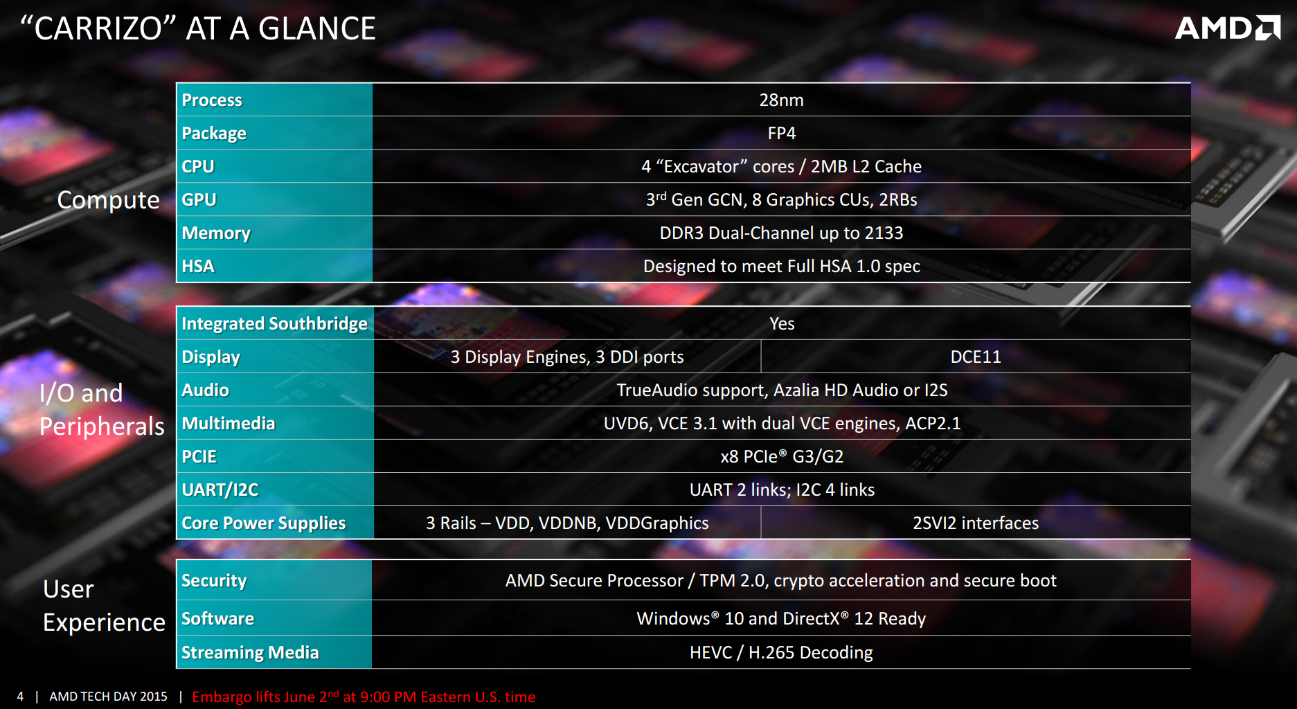
On a high level, Carrizo will be made at the 28nm node using a similar silicon tapered metal stack more akin to a GPU design rather than a CPU design. The new FP4 package will be used, but this will be shared with Carrizo-L, the new but currently unreleased lower-powered ‘Cat’ core based platform that will play in similar markets for lower cost systems. The two FP4 models are designed to be almost plug-and-play, simplifying designs for OEMs. All Carrizo APUs currently have four Excavator cores, more commonly referred to as a dual module design, and as a result the overall design will have 2MB of L2 cache.
Each Carrizo APU will feature AMD’s Graphics Core Next 1.2 architecture, listed above as 3rd Gen GCN, with up to 512 streaming processors in the top end design. Memory will still be dual channel, but at DDR3-2133. As noted in the previous slides where AMD tested on DDR3-1600, probing the memory power draw and seeing what OEMs decide to use an important aspect we wish to test. In terms of compute, AMD states that Carrizo is designed to meet the full HSA 1.0 specification as was released earlier this year. Barring any significant deviations in the specification, AMD expects Carrizo to be certified when the final version is ratified.
Carrizo integrates the southbridge/IO hub into the silicon design of the die itself, rather than a separate on package design. This brings the southbridge down from 40nm+ to 28nm, saving power and reducing long distance wires between the processor and the IO hub. This also allows the CPU to control the voltage and frequency of the southbridge more than before, offering further potential power saving improvements. Carrizo will also support three displays, allowing for potentially interesting combinations when it comes to more office oriented products and docks. TrueAudio is also present, although the number of titles that support it is few and the quality of both audio codecs and laptop speakers leaves a lot to be desired. Hopefully we will see the TrueAudio DSP opened up in an SDK at some point, allowing more than just specific developers to work with it.
External graphics is supported by a PCIe 3.0 x8 interface, and the system relies on three main rails for voltage across the SoC which allows for separate voltage binning of each of the parts. AMD’s Secure Processor, with cryptography acceleration, secure boot and BitLocker support are all in the mix.


137 Comments
View All Comments
VeixES - Wednesday, June 3, 2015 - link
Some OEM needs to pick this up fast.Carrizo based "NUC" device with HDMI2.0 output with more barebones approach than intel to reduce the cost of entry.
gostan - Wednesday, June 3, 2015 - link
Anandtech - AMD's marketing arm.bloodypulp - Wednesday, June 3, 2015 - link
Dumbest thing I've heard yet today.jabber - Thursday, June 4, 2015 - link
Everyone knows AMD has never had a marketing arm. That's why no one buys em.Seriously, the OEMs have moved on. Why bother with AMD when Intel sells because the average consumer has heard of Intel? Price doesn't come into it.
watzupken - Thursday, June 11, 2015 - link
To gostan, I find your comment above baseless and unconstructive to be honest. One article on AMD means AMD marketing arm. So what does that make you then?l_d_allan - Wednesday, June 3, 2015 - link
My impression is that it will be difficult (almost impossible?) for AMD to compete with a 28nm part against Intel's 14nm parts.And I think the next "tick tock" from Intel will be 10nm. Or not?
Novacius - Wednesday, June 3, 2015 - link
It'll be a tick, codenamed Cannonlake. But i don't expect it before the end of 2016/beginning of 2017.The_Assimilator - Wednesday, June 3, 2015 - link
Which will still be before AMD gets to 14nm.cjs150 - Wednesday, June 3, 2015 - link
Finally AMD release a reasonably power efficient chip.At 15W this is perfect for a passively cooled HTPC with 4k capability built in. I appreciate the HTPC market is small, but AMD have something that potentially (will reserve judgment until it is out and tested) beats everything Intel have comprehensively.
The problem for AMD will be that people like me already have a HTPC (in my case using i7-3770T which is overkill) and until the world moves to 4K there is no need to upgrade but if they produced something the size of Intel NUC but passively cooled I would be very tempted
watzupken - Wednesday, June 3, 2015 - link
I think this makes a very interesting APU. In fact, the most interesting APU from AMD to date. Unfortunately, it may not reach the shores from where I come from. It is either limited availability or the distros are not interested to carry in due to them expecting a low demand.